Deeds Demos (2)
Sequential Networks (Deeds-DcS)
(click on the figure of interest to open the corresponding example)
Flip-Flop Set-Reset (NAND version)

Shift Register (4-bits, E-Pet Flip-Flops)

Shift Register with feedback (16-bits)
Two 'Serial Input - Parallel Output' Shift Registers rotate a 16-bit pattern:

Universal Shift Register (circularly connected, 8-bits)
The 'Universal' Shift Register can load and rotate a 8-bit pattern:

Another Universal Shift Register (circularly connected, 16-bits)
The two 'Universal' Shift Registers connected to rotate a 16-bit pattern:

Parallel Shift Register (8-bits data)
The network shifts to right a parallel word of 8 bits. The 4-way Bus Multiplexer allows to select the delay of the output data (1, 2, 3 or 4 clock cycles), depending by the setting of S1 and S0.

In the Timing Diagram Window, a useful test sequence is already defined to verify the circuit behavior:

Synchronous Binary Up Counter (3-bits)
Synchronous Binary Up Counter, based on three JK flip-flops:

Synchronous Binary Up Counter with Enable (4-bits)

Synchronous 8 Binary Up/Down Counter with Enable
Normal and bus version:

Synchronous Cyclic Binary Down Counter (8-bits), Modulus 32
When the counter reaches zero, it reload itself with the value 31 (hex 1F):

Synchronous Cyclic Binary Up/Down Counter (16-bits), with Enable

Synchronous One-Shot Timer (8-bits)
When Start is pressed, PULSE is activated until the counter reaches zero.
Time dip-switches define the duration Tp of PULSE: (Tp = Time * Tck).

Synchronous One-Shot Timer (using a component from the library)
When Load is activated, the One-Shot Timer is loaded with N-1; when Load is released, it starts to count internally until it reach zero, activating TC (Terminal Count). The number N is defined using the properties dialog of the component (see the figure on the right side).


Cyclic Timer used as clock pre-scaler
The counter ECnt4 is enabled when the Cyclic Timer reaches zero. The duration of the Timer Cycle is defined in the properties dialog of the timer and, in this example, it is set to 32 clock cycles.

Digital Signal Generator (16 samples, 4 bits)
This simple Digital Signal Generator use a 4-bits counter to generate cyclically the addresses of a ROM memory. The samples of the sine wave will be generated sequentially on the ROM data outputs, and then decoded. The outputs of the 4-16 decoder will show a light moving like a pendulum.

The ROM has been programmed, at design time, with the samples of one period of a sine wave, using the Rom Editor/Programmer, available in the context menu of the component:
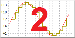
 Graphically, the samples:
Digital Signal Generator (16 samples, 4 bits), with Digital to Analog Converter
This generator is similar to the previous one, but the output is given by a DAC component:

The ROM has been programmed, at design time, with the samples of one period of a sine wave, using the new Waveform Editor (available in the Rom Editor/Programmer):

Digital Signal Generator (256 samples, 8 bits)
This Digital Signal Generator uses a BUS-type wiring, a bigger capacity ROM, and an eight-bits DAC:

In the Waveform Editor, a wave has been defined as Fourier Series, truncated to the third harmonic:

Ram Memory Test Circuit (16 x 4)
This Random Access Memory component (16 cells x 4 bits) is enabled by the CS (Chip Select) input. When WR (Write) is low, the memory is read: the content of the cell currently selected by the A3..A0 address lines is available on the outputs R3..R0. When WR (Write) is high, the inputs D3..D0 are copied in the cell currently selected and the new data is also visible on the outputs R3..R0; finally, when WR (Write) returns low, the new data is latched in the cell. On start, all the RAM contents are not defined yet, and the simulator returns "unknown" values on the R3..R0 outputs.

A "Minimalist" CPU
A demonstrative 8-bits CPU, with a choice of test programs and notes, by Jérôme Lehuen (University of Le Mans, France).