Synchronous Serial Transmitter (4 bits)
In this example, we’ll design a simplified 4-bits synchronous serial transmitter:
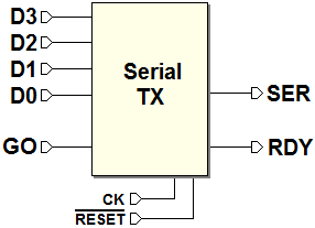
The unit reads a 4-bits parallel data (D3…D0); when the input GO makes a transition from 0 to 1, data is serialized and transmitted on the line SER, in the format of a serial packet, as in the following figure:
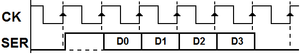
- The bit sequence is synchronous with the clock CK;
- The bit time duration is equal to one clock cycle;
- Each sequence begins with a Start Bit (high);
- Four data bits follow (D0, D1, D2 and then D3);
- The bit packet ends with a Stop Bit (low).
The transmitter will insert sequentially the D0, D1, D2 and D3 values on the line SER, after the transmission of the start bit. One stop bit is then generated, simply maintaining the SER line at 0 for the duration of a clock cycle. The output RDY is activated only when the transmitter is in the idle state (i.e, when it is not transmitting, waiting for a low to high transition on the input GO).
Solution
We divide the circuit into a structure Controller + Datapath. We need to transmit, sequentially:
- a high level;
- the four bits D0..D3, starting from D0;
- a low level;
- the idle state of the line (i.e. we'll continue to generate a low level, during the waiting for the next GO command).
To do this, we use the 'Mux 8-1' multiplexer (from the Deeds library), to select the source to be sent to the output, under the control of the selection lines S2..S0:
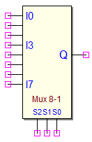
As shown in the next figure, we connect the multiplexer inputs in the following order:
- I0 = low (i.e. the line idle state value);
- I1 = high (the start bit value);
- I2..I5 = D0..D3 (the data bits, in the requested order);
- I6 = low (the stop bit value);
- I7 = low (even if this will be not used).
The multiplexer output could be directly connected to the output SER but, to grant the synchronicity of the output respect to the clock CK, it is better to insert a D-PET type flip-flop into the data path. In this mode, we’ll be sure to cut away hazards and unmatched delays (a click on the figure will open the circuit in the Deeds-DcS):

The controller will wait for the GO command, activating the RDY output and setting S2,S1,S0 = 000, to drive the output flip-flop with the idle state level (low). When the low to high transition on GO is detected, on the next clock cycles we’ll select, in order, the other multiplexer inputs, to send the packet bits (a click on the figure will open the ASM chart in the Deeds-FsM):

The timing simulation, reported in the following figure, shows that the system behaves correctly:

At the beginning data is set (D0=0, D1=0, D2=1 and D3=1). Then, GO is activated, commanding the generation of the serial sequence. At every clock cycle, the S2..S0 selection changes, sending to DSER (the input of flip-flop) the correct bit value, to compose the serial sequence. Note that the output SER shows the same sequence, but delayed –as expected- of one clock cycle.
NB: the figure above has been obtained using the Deeds-DcS timing diagram, via the command indicated in the following screenshot: