|
|
||||||||||
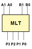
| Design the two-bits binary multiplier shown in the figure. The multiplier receives two unsigned numbers A and B (coded as two-bits binary numbers, on the inputs A1,A0 and B1,B0), and generates the number P (coded as four-bits binary number, on the outputs P3, P2, P1, P0). The number P is the product between the number A and B.
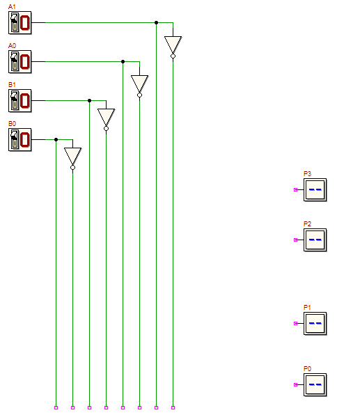
Write a truth table of the binary multiplier. Compile a K-maps for each output and write the expressions of the minimized synthesis of each output (synthesize them as two-level AND-OR networks). Draw the schematic of the resulting network, using (as a trace for the solution) the d-DcS schematic template provided here (click on the figure below): Verify the circuit behaviour
through a functional simulation | |||||||||||


 and a timing simulation
  (a suitable test sequence is available in the Timing Diagram window).