|
|
||||||||||
| Design a synchronous digital system in charge of receiving commands through a serial-line and, consequently, generating pulses whose time duration depends on the received data. The received data, on the LN input, is represented by three bits, D0, D1 and D2, packed together with a start bit (at ‘1’) and two stop bit (at ‘0’), according to the following figure.
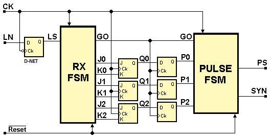
The input LN changes its value synchronously with the rising-edge of the clock CK. The figure shows the architecture of the system, composed by two FSM's and a few flip-flops.
The D-net flip-flop, visible on the top-left corner, re-synchronizes the input data stream, on the falling-edge of the clock CK. The RX FSM is in charge of receiving and decoding the re-synchronized data stream. Each time the RX FSM receives a new data stream packet, the information bits received are stored on three JK-pet flip-flops (D0 is stored on Q0, D1 on Q1, and D2 on Q2). If the received sequence is valid (i.e. the two stop bits are '0'), the RX FSM activates, for the duration of one clock cycle, the signal GO. The other three D-pet flip-flops (P0, P1 and P2) are in charge of copying the information received, on the rising edge of the GO signal. This is useful, because in this way the receiver is immediately free to receive a new input sequence, as soon as the data has been copied from the JK flip-flops to the other ones. The PULSE FSM waits for the GO signal: when GO is activated, it starts, activating the output PS. The duration T of the pulse, in clock cycle units, is a function of the signals P1 and P0, and it is defined as T = (2 + P1P0), were P1P0 is a binary number (P1= MSB, P0=LSB). On the last clock cycle of the output pulse PS, if the signal P2 is high, the PULSE FSM generates SYN, to warn that pulse generation is terminating. The asynchronous !Reset input forces the system in an idle state, waiting for a start bit on LN. First, you should design and simulate the RX FSM. Then design and simulate the other one, PULSE FSM. Once the two machines are completed, draw the schematic of the whole system, importing the two FSM components in the d-DcS. You can use the d-FsM ASM diagram templates provided, for the RX FSM and the PULSE FSM, as well as for the d-DcS whole system. Finally, simulate the whole system with the d-DcS timing simulator (suitable test sequences are available in the Timing Diagram window).
| |||||||||||


