|
|
|||||||||
| The serial line receiver will expect a signal, from the line LINE_IN, as the one described in the following figure:
The 10 bit packet is composed as follows:
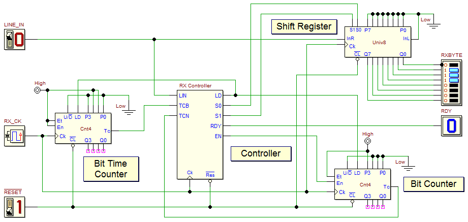
The next figure shows the receiver, based on a Finite State Machine as controller (click on the figure to open the schematic in the d-DcS editor): The system is composed of a Bit Time Counter, a Shift Register, a Bit Counter, and a Controller.
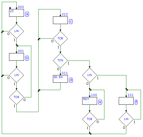
The controller clock frequency is 16 times the bit rate of the received packet. To catch the Start Bit, the controller samples its input LIN (alias LINE_IN) at every positive clock edge, in state (a). When LIN goes high, the controller continues to sample it, at the same rate, in state (b). If LIN is sampled always high, until the middle of the bit time is reached, the controller declares valid the Start Bit, and goes in state (c). On the contrary, if LIN returns to low, operations are restarted, looking again for a next valid start bit, in state (a). Note that the middle of the bit time is signaled by the TCB line, that is generated by the Bit Time Counter. This one is initialized, by means of the LD line, in state (a), to the starting value '0110'. As a result of this initialization, the first occurrence of TCB is generated on the middle of the bit time; the next occurrences, instead, will be generated every bit time (i.e. every 16 clock cycles, the counter module). The controller checks TCB also in state (c), to synchronize the operations of the Shift Register. When TCB goes high, the controller sets S0 = '1' and S1 = '0', in state (d), causing the LINE_IN data acquisition (on InR of the Univ8 component) and the right shift of all the other bits of the register. This couple of states (c,d) is repeated 8 times, i.e. until TCN is activated. TCN is generated by the Bit Counter when it reaches '0000', i.e. when the received data bits are over. Note that the Bit Counter is decremented, by means of EN, in state (d), each time a bit is acquired in the shift register. The next task of the algorithm relates to the Stop Bit validation. In state (c), when TCB is activated, but all the data bits have been received (TCN = '1'), instead of acquiring the Stop Bit in the shift register, the controller checks directly its value. If the Stop Bit is zero, the packet is assumed valid, and the RDY signal generated, in state (e), for the duration of a bit time. Otherwise, if the Stop Bit is high, the received data bits will be ignored (because the RDY signal is not generated) and the algorithm will re-start from state (a). The loop state (f) is a simple attempt to recover the error state due to the wrong stop bit. In state (f) the controller waits for a low value on LIN, before to catch the next start bit (although this solution couldn't be the better one to handle a wrong stop bit reception). You can test the circuit using the d-DcS simulator, in Animation Mode | ||||||||||


 Bit Time Counter
 and in Timing Mode
  . A proper test sequence is available in the timing simulation window.