|
|
||||||||||||||||||
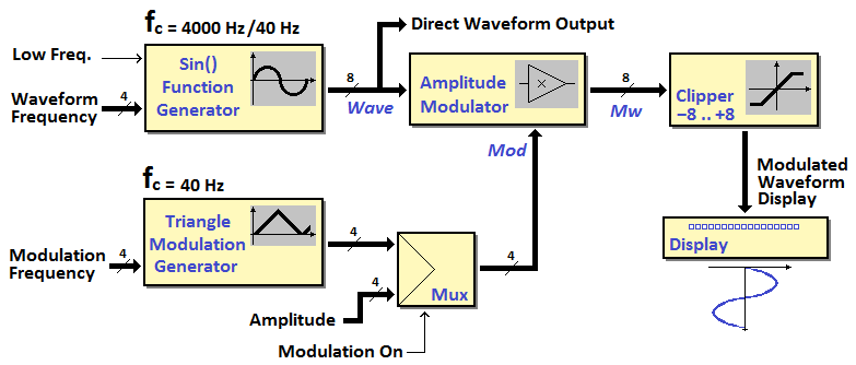
| In this laboratory you are asked to complete the design of a Digital Waveform Generator, based on a microcomputer. After verification by simulation of the project, we will realize a prototype on FPGA to verify its operations. The system architecture is shown in the next figure:
The block in the upper left corner represents the generator core, which produces a sine wave using a pre-computed table, producing a sample of 8 bits every 0.25 mS (i.e. at a sampling frequency fc = 4 kHz). A numeric input (Waveform Frequency, 4 bits) allows you to set the frequency f of the sine wave, according to the relation: f = wf (fc / 256), where wf is the input number. We can therefore generate frequencies between 0 and 234.4 Hz, in steps of 15.625 Hz. If the test input Low Freq is activated, fc is reduced to 40 Hz, and the range is scaled down by a factor of 100 (between 0 and 2.34 Hz). The generation method used here consists in the calculation of phase angle d reached at each sampling instant. The round angle is divided, for convenience of calculation, in 256 parties, and at every sampling instant, the phase angle d is increased by the input amount wf. The calculated d angle (0..255) is then used as an index into a table of values, that provides us with the corresponding value of sin() function. For symmetry reasons, the table contains only the values of the positive half-wave, and is indexed from 0 to 127. The other half of the sinusoid is obtained from the first, by complementing the values of the table. The Modulation Generator works similarly, as regards the calculation of phase angle. However, given that we generate a triangular waveform, it is not necessary to resort to a table, and its values are obtained proportionality from the phase angle. The generator produces a positive sample, coded on 4 bits, every 25 mS (namely, with a sampling frequency of 40 Hz), and calculates the phase angle in 1024 parts of the round angle. Even here, a numeric entry (Frequency Modulation, 4 bits) allows you to set the frequency f, according to the relation: f = mf (fc / 1024), where mf is the number in input. The frequency range results between 0 and about 0.59 Hz, in steps of 0.039 Hz. The Amplitude Modulator allows to attenuate the values of the sine wave by a positive multiplicative coefficient (4 bits), the value of which is generated, by user choice, by the Modulation Generator, or from the input Amplitude. The selection is controlled by the input Modulation On. The relation between input and output of the modulator is Mw = Wave (Mod / 256), where Mw is the output signal, Wave is the signal that comes out of the sin wave generator, and Mod is the modulation signal. The Clipping stage that follows (the Clipper) has the purpose of limiting the signal amplitude to values between -8 and +8. Our implementation of the system is based entirely on a microcomputer, programmed to realize, with interrupt techniques, the individual blocks described before. We are using an architecture for general purposes, such as that of the microprocessor DMC8, as a Digital Signal Processor (DSP).
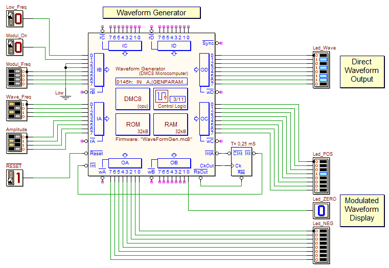
You see in the figure, from above and from the left side:
In the figure is also visible, on the right side of the microcomputer, a Interrupt Timer component, set for interrupt cyclically the microprocessor. To better understand the description, it is useful to refer to the general structure of the program, that you can download here (the template is the less complete among the ones available below). After the necessary initialization of the stack, variables and interrrupts, the main program executes an infinite loop, which takes care of reading the input ports, in order to obtain information from the various switches, and encode it into appropriate variables, used by interrupt handler, such as the following:
Interrupt Program Specifications The interrupt program runs every 0.25 mS, by the interrupt timer, i.e. 4000 times per second. After the necessary internal registers saving on the stack, the program evaluates if 25 mS have elapsed (equivalent to 100 calls). a) If 25 mS have not yet elapsed, it checks whether the user require the reduction of the signal sampling frequency (in the variable SLOWFC): if yes, the interrupt program exits immediately, because all the evaluations will be carried out only every 25 mS (i.e. 40 times per second). Otherwise it proceeds, jumping forward to WAVE, with the generation and processing of the next sample, performing the following activities on each interrupt call (i.e. at the sampling frequency of 4000 Hz). b) Instead, if 25 mS have elapsed, before generating the next sample (at WAVE), a call is made to the subroutine MODGEN, which realizes the modulation generator, described later. At this point, at the label WAVE, the program executes the subroutine WAVEGEN, which realizes the main generator (described later); the generated value is written on the eight output lines Direct Waveform Output. We select the modulation value, before calling the subroutine of the amplitude modulator MULTIPLY. Depending on the user's request (in the variable MODUL), the modulation value may be equal to what is generated from the subroutine MODGEN, or to the contents of the variable AMPL. MULTIPLY performs a 8x8 bit multiplication between the signal value (in the range -127.. +127) and the amplitude control, then dividing the result by 256. The overall result is an attenuation of the signal generated by a factor equal to (A / 256). Before being displayed on the display, obtained with the 17 LEDs in a row (subprogram DISPLAY), the signal values are limited, by the subprogram CLIPPER, to the displayable range +8..-8. Finally, the routine ends with the restore of all registers previously saved, and interrupt are re-enabled. MODGEN (Modulation Waveform Generator) It calculates the triangular waveform that modulates the amplitude of the sinusoidal signal. The current phase angle is calculated on 10 bits, in MODPHASE (a 16 bits variable): it is obtained incrementing the variable, every 25 mS, with the amount contained in of the variable MODFREQ. The function value is then calculated by dividing by 64 the value of the phase angle. The value is directly this one if it is between 0 and 7, while if it is greater or equal than 8, we "reverse down" the curve (inverting the bits and adding 1), generating the "triangular" signal visible in the figure:
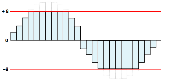
The generated value is stored in the variable MODAMPL. WAVEGEN (Main Waveform Generator) It generates the sinusoid samples, as described previously. The current phase angle is stored in the variable PHASE; the next angle is calculated by adding FREQ to the content of the variable PHASE. The current phase angle (0..255), masked to 7 bits, is then used as index into the table SINTABLE, which contains the values of the positive half-wave of the sinusoid. As written before, the other half of the sinusoid is obtained from the first, two-complementing the table values, if the phase angle is greater than 127. The current value of the sine wave is generated in the accumulator A. Note that the table is allocated in the memory (with the 'ORG 1000h') so that the high part of the address is always the same for all of its locations (to simplify the calculation of the address of the table items). CLIPPER (Signal Clipping) The Clipper prevents the values, coming from the modulator, may exceed the pre-defined limits (here -8..+8). It work on this binary number in the accumulator A, considering it as unsigned, and checking first that is between '11111000' and '11111111' (i.e. from -8 to -1), or between '00000000' and '00001000' (i.e. between 0 to +8). If it falls within those limits, returns to the caller without changing the number. Otherwise the the number exceeds the limits and must be reduced: to do this, it controls the sign (bit 7), and then replaces the number with '00001000' (+8) if it is positive, or with '11111000' (-8) if negative. The following figure shows an example of a signal whose excursion is reduced by the limiter:
DISPLAY (Signal Display on a LED bar) The value to be displayed is received in the accumulator A; the subroutine uses the table LEDTABLE to display only one LED at a time, the position of which matches the value of the signal. Note that each row in the table defines only one '1', corresponding to the LED that should be lit. The table has 4 bytes per row, so to use the value as an index into the table, it is multiplied by 4 to obtain the displacement from the table base address (also in this case the table is allocated so that the upper part of the address is always the same for all rows). Note that the label LEDTABLE defines the center of the table, and that the dislocation can be positive or negative, as the input number. The first byte defined in the table row is copied on the port that drives the eight LED located on the left side of the '0', and the second on the port that drives the '0' LED', the third to the port connected to the eight LEDs on the right side. MULTIPLY (Integer multiplication) The subroutine MULTIPLY realizes the amplitude modulator, multiplying the value of the signal (received in the register B), for the value of the modulation (received in the register A). The result is calculated, step-by-step in the register HL, used as 16 bit accumulator of the result. The subroutine, first of all, copies the value in B into the register DE (the multiplicand). To do this it is necessary to check the sign of B, which we extends to 16 bits (the upper part of the register DE must be cleared if the number is positive, otherwise it must be set to '11111111'). Then, it executes a loop that is repeated 8 times, i.e. for each bit in the register A (the multiplier). On every repetition, the multiplier A is shifted to the left and the bit that comes out is checked: if this is equal to '1', the multiplicand DE is added to HL (the partial result), otherwise not. In any case, before moving to the next loop repetition, HL is shifted to the left by one step. The procedure is similar to what we execute "by hand", on paper, but with three differences: 1) it starts from the leftmost bit of the multiplier, rather than from the right one, 2) it performs a partial sum on every step, instead of performing the total sum at the end and, 3) we scale the result to the left at every step, instead of "indenting" in diagonal, on paper, the individual results. The final division by 256 would correspond to right shift the register HL by 8 positions. It is easier and efficient to take directly, as result, the high part H, coping it in the register A (the return value of the subroutine). We should, also, to round the result to the nearest integer, rather than truncate it. To do this, we check the highest bit of the lower part of HL: if it is equal to '1', we increment the result by one unit. Here four templates are available for possible solutions, in assembly DMC8 code, in descending order of difficulty:
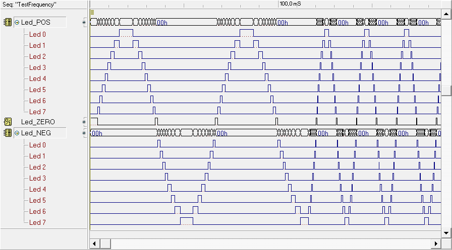
Who wants to deal only with the analysis of already written code, and the simulation and implementation on FPGA of the system, will find here a complete solution. At the end of the writing and the functional test of the program (in the d-McE), you must program the microcomputer ROM (you can open the schematic in the d-DcS by clicking here). It is recommended to use the provided schematic without to delete or change the input and output terminations, because they have been set for the export of the project on the FPGA board. In the d-DcS timing diagram window are available some appropriate test sequences. The sequence "TestFrequency" shows an analysis of the system without amplitude modulation, by setting different frequencies in the sine wave generator. As you can see, it is possible to observe the LED pattern, which follows the sinusoidal shape:
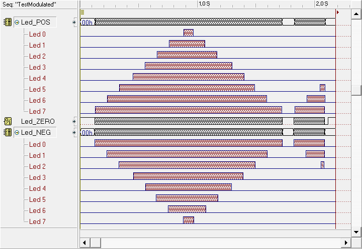
The sequence "TestModulated" shows the analysis of the system with the amplitude modulation triangular, without varying the frequency of the main generator. As you can see, it is possible to observe the time course of the signal generated, which follows a triangular envelope:
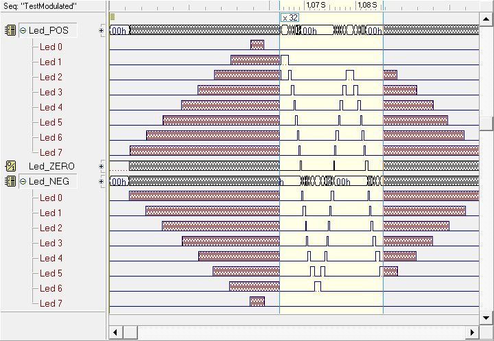
The following figure shows the same result but, thanks to the use of the "magnifier", we have, in addition to the overall view of the envelope of the signal generated, also a close-up view of the signal (in the enlarged time interval), where we recognize its sinusoidal shape:
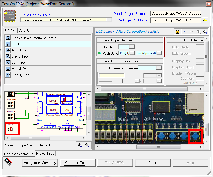
Now we go to the physical implementation of the project in the FPGA board. The general procedure is described in the introductory tutorials: The "Test on FPGA" command of the d-DcS will open the following dialog window:
All the needed associations between d-DcS schematic and the FPGA board input/outputs are already set in the given schematic. To optimize the experiment as described on the FPGA board, we highlight the associations, in a summarized way, even in the figure below (the "control panel" of our system):
| |||||||||||||||||||


