|
|
|||||||||||||||
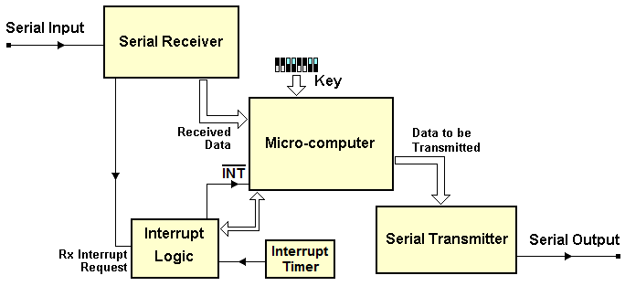
The following device is an asynchronous serial data processor, in charge of receiving serial sequences, processing and re-transmitting them. The architecture of the system is based on an embedded microcomputer and some application-specific hardware. In this project, you'll write part of the assembly code to program the embedded microcomputer, following the given specification. Finally, you'll carry out and test a prototype of the system on an FPGA board. The system is represented, as functional blocks, in the following figure: Serial Receiver operationsThe serial receiver is in charge of receiving asynchronous serial data packets as the one described in the following figure:
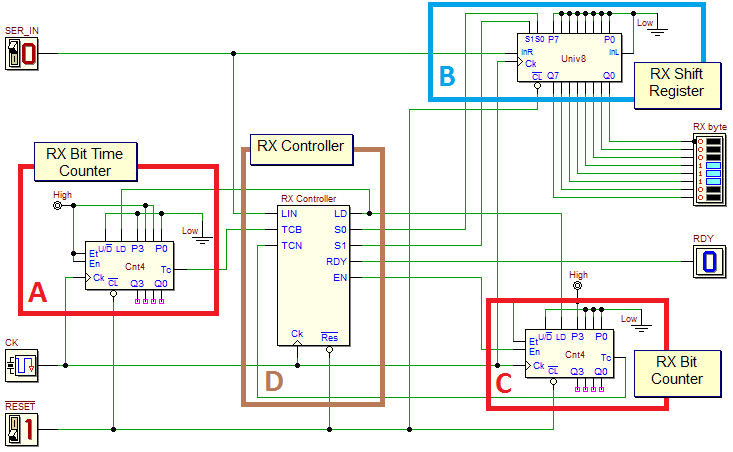
The data packet is composed of a START bit at '1', followed, in order, by the bits D0, D1, D2, D3, D4, D5, D6 and D7, and finally terminated by a STOP bit at '0'; the "bit time" is equal to 1.6 µS, corresponding to 625 Kb/s (10 MHz /16). The next figure shows the serial line receiver (click on the figure to open the schematic in the editor): The system is composed of the RX Bit Time Counter [A, highlighted in red], on the left hand side of the figure, the RX Shift Register [B, in blue, top-right], the RX Bit Counter [C, in red, on the right], and the RX Controller [D, in brown, based on a finite state machine].
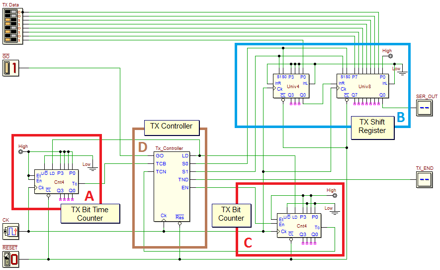
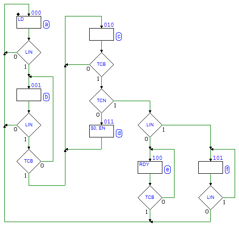
The controller clock frequency is 16 times the bit rate of the received packet. To catch the Start Bit, the controller samples its input LIN (alias SER_IN) at every positive clock edge, in state (a). When LIN goes high, the controller continues to sample it, at the same rate, in state (b). If LIN is sampled always high, until the middle of the bit time is reached, the controller declares valid the Start Bit, and goes in state (c). On the contrary, if LIN returns to low, operations are restarted, waiting again for a next valid start bit, in state (a). Note that the middle of the bit time is signaled by the TCB line, that is generated by the RX Bit Time Counter. This one is initialized, by means of the LD line, in state (a), to the starting value '0110'. As a result of this initialization, the first occurrence of TCB is generated on the middle of the bit time; the next occurrences, instead, will be generated every bit time (i.e. every 16 clock cycles). The controller checks TCB in state (c) too, to synchronize the operations of the RX Shift Register. When TCB goes high, the controller sets S0 = '1' and S1 = '0', in state (d), causing the SER_IN data acquisition (on InR of the Univ8 component) and the right shift of all the other bits of the register. This couple of states (c,d) is repeated 8 times, i.e. until TCN is activated. TCN is generated by the RX Bit Counter when it reaches '0000', i.e. when all serial bits have been received. Note that the RX Bit Counter is decremented, by means of EN, in state (d), each time a bit is acquired in the shift register. The next task of the algorithm relates to the Stop Bit validation. In state (c), when TCB is activated, but all the data bits have been received (TCN = '1'), instead of acquiring the Stop Bit in the shift register, the controller checks directly its value. If the Stop Bit is zero, the packet is assumed valid, and the RDY signal is generated, in state (e), for the duration of a bit time. Otherwise, if the Stop Bit is high, the received data bits will be ignored (because the RDY signal is not generated) and the algorithm will re-start from state (a). The loop around state (f) is a simple attempt to recover the error state due to the wrong stop bit. In state (f) the controller waits for a low value on LIN, before to catch the next start bit (although this solution is not the best one to handle a wrong stop bit reception). You can test the circuit using the d-DcS simulator, in Timing Mode Serial Transmitter operationsThe serial transmitter serializes the given parallel data (8 bits) in asynchronous serial data packets composed of 10 bits. The format is the same of the receiver. The next figure represents the transmitter (click on the figure to open the schematic in the editor). The system is composed of the TX Bit Time Counter [A, highlighted in red], on the left hand side of the figure, the TX Shift Register [B, in blue, top-right], the TX Bit Counter [C, in red, on the right], and the TX Controller [D, in brown, based on a finite state machine].
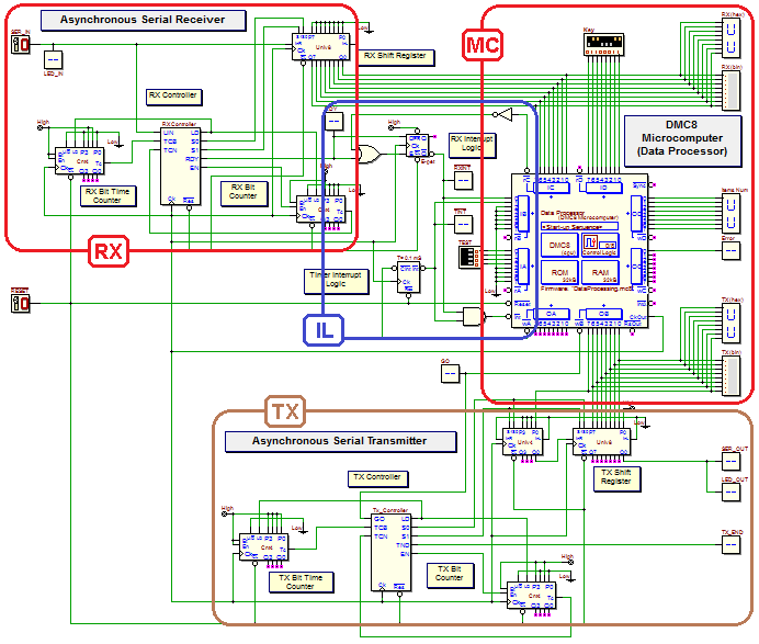
The !GO input starts the transmission: the first two states (a) and (b) are in charge of waiting for the pressure of the push-button ("low" when pressed) and also to activate LD, to preset all the counters. In the state (c), the activation of S0 and S1 loads the parallel data in the TX Shift Register, while EN causes the decrement of the number of bits to be transmitted. In the state (d), the controller waits for a TCB signal from the TX Bit Time Counter: when it occurs (every 1.6 µS), the controller activates (e) the right shift of the data register (S1 = '0', S0 = '1') and decrement the number of bits to be transmitted (EN = '1'). When the number of bits to be transmitted becomes zero (TCN = '1'), the controller reaches state (f), where it generates the TND output, to signal the transmission end. Finally, the controller returns to state (a). You can test the circuit using the d-DcS simulator, in Timing Mode The systemIn the next figure is represented the schematic of the whole system (click on the figure to enlarge it in another window): This figure is quite complex, so we have marked, in color, four functional areas. The serial receiver [RX] and the transmitter [TX], that we analyzed before, are clearly recognizable; likewise, the microcomputer [MC] . The fourth area, the interrupt logic [IL], includes one E-PET flip-flop, an Interrupt Timer and a few logic gates. Microcomputer operationsThe DMC8 microcomputer reads the data parallelized by the serial receiver, process it, and then sends the results to the transmitter. IC port reads the 8-bits data coming from the receiver. ID port reads a Key, user-defined by means of dip-switches, that will be used to encrypt data, before re-transmission. IB port is used to test interrupt request, and IA port reads a group of switches to set a few test modes, as explained later. OA port allows to reset the timer interrupt request. OB port sends the data to the transmitter. OC port is connected to the Error output line. OD port is used only for test. The receiver, when a new data packet has been de-serialized, sends an interrupt request to the microcomputer, that will read the data through IC port. The received byte is temporary stored in the microcomputer RAM, in a circular queue (explained below), awaiting to be processed and re-transmitted. If, during the system operations, the queue had no more space to contain the incoming data, the system will activate the line Error. Since this is considered a serious system fault, the error condition, once activated, can be cleared only by restarting the system manually. The Interrupt Timer is set to request microcomputer service every 0.1 mS. When interrupted by the timer, the microcomputer checks if the circular queue contains data to be transmitted: if so, it picks up a byte from the queue, encrypts and send it to the serial transmitter, writing the OB port. For test, the number of bytes to be transmitted, awaiting in the queue, is reported on an hex display connected to the OD port. The microcomputer encrypts data by making a simple bit-by-bit EXOR between received data and the Key (so, if Key is zero, no modification is done on the data). The Circular QueueA queue is a kind of data structure, were data is handled in a "First In First Out" (FIFO) mode: the element we "queue" first is the first that we will "de-queue". In this application, we use a queue to store data as they arrive, and then re-transmit them on a regular base. If data arrive more quickly than they are re-transmitted, the queue gradually fills; then it empties regularly when the incoming data rate slow down or end. Note that queue length is not infinite, so we could fill it up, having no space anymore to store incoming data. We use a pointer ('IN_ptr') to address, in the queue buffer, the first location to write with the incoming data. After we queue a new byte, the 'IN_ptr' pointer is incremented to address the next location to write. The queue is "circular": when we write the last buffer location, the pointer is "circularly" reset to the first one. The 'OUT_ptr' pointer addresses, instead, the first byte to be de-queued. After we pick up a byte, it formally disappear from the queue, and the 'OUT_ptr' is incremented to address the next location to get. Also in this case, when we read the last buffer location, the pointer is reset to the beginning of the buffer. In the example of the next figure, four bytes have been added to the queue: 'IN_ptr' points the next location to write, while 'OUT_ptr' points to the first byte to be de-queued.
In a sense, we can say that the 'OUT_ptr' chases the 'IN_ptr': the queue is empty when 'OUT_ptr' reaches 'IN_ptr'. When they are different, as in the previous figure, some data need to be de-queued and then transmitted. When the pointers are equal, no more data is there (see the following figure).
Note that a special case needs to be managed, because the "empty queue" condition could be confused with that of "queue full". To avoid this ambiguity, we consider the queue "full" when the 'IN_ptr' addresses the empty location before the one addressed by the 'OUT_ptr', as in the example reported in the next figure. In this way, we sacrifice a location in the queue, but avoid to introduce other variables.
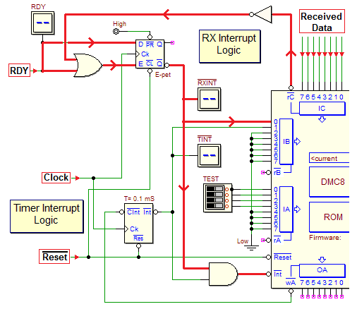
Interrupt LogicIn the following figure, a part of the interrupt logic is highlighted. A E-PET flip-flop is set when the receiver activates RDY (signaling that a new data packet has been received). The activation of the flip-flop !Q output (displayed as !RXINT) will interrupt the microcomputer, through the AND gate, activating its interrupt request !Int input. The flip-flop !Q output is connected also to bit 0 of IB port, so that the interrupt handler routine could recognize the receiver as the device that requested interrupt. Moreover, the !rC strobe of the IC port, through some logic gates, is connected to the flip-flop E input: when the received data is read on IC port, the flip-flop is automatically cleared and the interrupt request cancelled.
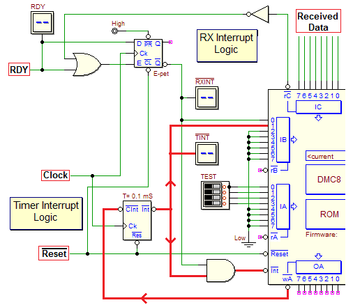
The transmitter interrupt logic, highlighted in the next figure, is different. The cyclic activation of the Interrupt Timer output grants the periodic re-transmission of the bytes, if any is present in the queue. The Interrupt Timer output, displayed as !TINT, is connected (through the AND gate) to the microcomputer interrupt request !Int and to the bit 1 of IB port, so that the interrupt handler routine could recognize the timer as the interrupting device. To clear the timer interrupt request, the microcomputer writes the OA port (by writing the port, we activate the !wA strobe, independently of the byte value).
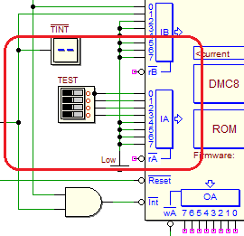
Test ModesThe next figure highlights the 4-switches TEST component, connected to the IA port, that allow to set a few test modes, useful to verify the data queue functionality.
The following table define the functionality of the TEST switches:
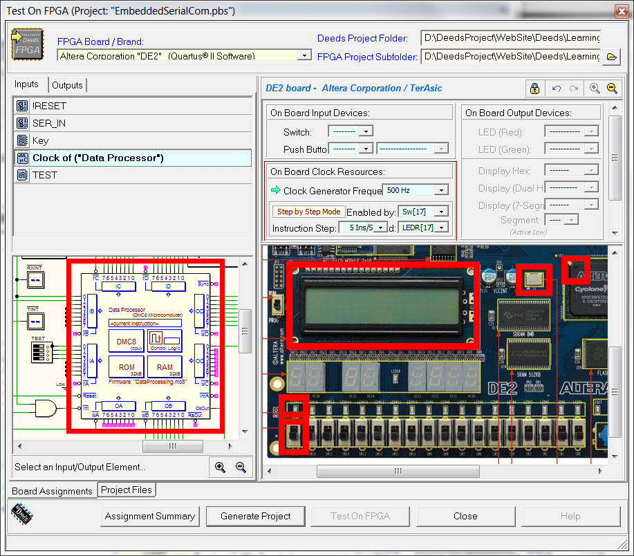
When the "Transmitter Auto Send Mode" is set, at every timer interrupt request, without regard to the queue contents, the transmitter is forced to transmit a test value. The byte value starts from '11111111' and decrements by one after every test transmission. If "Transmission inhibited" is set, no data is picked up from the queue and no transmission is executed. Setting this mode inhibits also the "Transmission Auto Send Mode", if set. In the "Discard Received Data Mode" is active, data coming from the serial receiver is ignored, and not inserted in the queue. When the "Receiver Auto Fill Mode" is set, at every timer interrupt request, a new test byte is generated and added to the queue, as it were received from the serial line. The byte value starts from '00000000' and increments by one after each insertion in the queue. AssignmentAccording to the above specifications, write the assembly program that will be loaded into the DMC8 microcomputer. After writing and functionally testing the program (in the d-McE), you must program the microcomputer ROM (you can open the schematic in the d-DcS by clicking here). It is recommended to use the schematic provided without deleting or changing the input and output terminations, because they have been set for the export of the project on the FPGA board. In the d-DcS timing diagram window are available some appropriate test sequences. Here three solution templates are available, to be completed, in assembly DMC8 code, in descending order of difficulty. In the first file, the most challenging, the general structure of the solution is there, including symbol definitions, variable initializations, basic interrupt handling and a few subroutine to handle the queue. The user must code the receiver and transmission modules, organized into sub-programs, and add all the additional instructions useful to test the system. The second partial solution adds to the previous one the realization of 'RXDATA', that inserts the received data in the queue. The third file adds also the module 'TXDATA', that picks up and re-transmits data from the queue; only the test code is to be written. To deal only with the analysis of completely written code, and the simulation and implementation on FPGA of the system, find here a complete solution. Here we begin the procedure for the physical implementation of the project in the FPGA board. The general procedure is described in the introductory tutorials: The "Test on FPGA" command of the d-DcS will open the following dialog window:
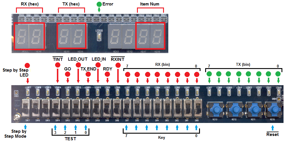
The associations between the d-DcS schematic and the FPGA board (inputs and outputs devices), have been already defined, so you do not need to change them. The microcomputer clock is set to 500 Hz (rather than 10 MHz), to allow visual examination of the behavior of the system. The "Step by Step Mode", set as shown in the figure above, will be activated at run time by the switch SW[17], and it is defined to work in automatic (executing 5 instructions per second). To optimize the testing of the system on the FPGA board, associations are highlighted in a summarized way in the figure below (the "control panel" of our system):
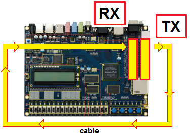
To test the system we need to use one or more separate boards, interconnected by means of appropriate cables. We connect them using the two 40-pin connectors available on each board, joined with a two-wires cable. The serial output SER_OUT is generated from pin 1 of the GPIO_1 connector, and the serial input SER_IN is received on pin 2 of the GPIO_0 (see the connection schematic). If we have one board only, we connect the cable between the two connectors available in the board (as shown in the next figure): the serial transmitter, set in "auto-send" test mode, generates the data packets that, through the cable, return to the receiver of the same system.
If more boards are available, it is interesting to interconnect them as suggested in the following figure. Setting the serial transmitter of the board 'A' in "auto-send" test mode, we'll send data to the board 'B', that will re-send processed data to the board 'C', and so on. Combining various test modes on each board, it is possible to test extensively the system behavior (i.e. to fill temporary the queue of a board, and then let it empty again).
Be extremely careful in placing and removing the cables, to avoid mechanical damage to the connector pins. To avoid possible damage to the FPGA chip, whose pins are directly connected to the connector, it is necessary to carry out this operation when power is off. | ||||||||||||||||



 RX Bit Time Counter [A]
 . Some test sequences are available in the timing simulation window.