|
|
||||||||||
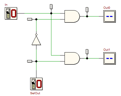
| Verify the behavior of the 1->2 demultiplexer represented in the figure below, using the Deeds Digital Circuit Simulator (d-DcS). Click on the figure to open in the d-DcS a trace of the network's schematic, and then complete it to obtain the schematic below: While completing the drawing, you should also name the Input and Output components
(click on the properties command The test sequence shown below is available in the Timing Diagram window: in this sequence, the input In changes its value continously. It is easy to verify that the value of SelOut selects which of the two outputs (Out0 or Out1) will copy the In variations. The output not selected will remain at '0'.
| |||||||||||


 on the d-DcS tooolbar, then click
on each Input and Output component to be named). Once completed the schematic, you'll be ready to start a functional
simulation of the network
  , and then a timing simulation
  .
. 