|
|
|||||||||||||||
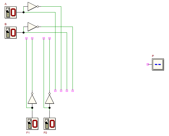
| Design a logic network acting as programmable logic gate. The network has four inputs A, B, F1, F0, and one output P. The output will take the value of the functions NAND, NOR, EXOR of A and B, accordingly to the combination of the control variables F1 and F0. The relation is:
Assume that the combination F1, F0 = 11 is never applied to the inputs. You are requested to produce the following items:
Draw the schematic of the resulting network using the following schematic to be completed (click on the figure to open it in the d-DcS): First, check the correctness of your design using the functional simulation
| ||||||||||||||||


 .
When done, simulate the net also with the timing simulator
  . We suggest to use the test sequence shown below (available in the Timing Diagram window):