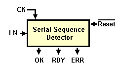
| The following digital system is a serial
sequence detector. It receives the serial line LN, and generates three outputs signals (OK, RDY and ERR):

The input LN receives a synchronous
bit stream consisting of 5-bits packets (see the next figure):

The line input LN is at value '0' while the system waits for a packet. Two packets are separated
by at least three clock cycles. The start (first) bit of each packet is always '1' and the stop (fifth) bit should be '0'.
They carry no information, but are used by the system to recognize the
data in the stream. The second, the third and the forth bits (B0, B1 and B2),
instead, carry the information data. Each bit has a fixed duration, called bit-time. In this case, the bit-time is equal to one clock cycle, and the clock positive edge samples data in the center of the bit-time.
The system waits for the start bit. Then, it receives and processes, one by one, all the bits of the packet. The detector is in charge of recognizing the input sequence B0, B1, B2 = '0', '1', '1', according to the following specifications:
- If, at the end of the packet, the stop bit is not '0' (i.e. the packet has not been received correctly), it sets the output ERR for the duration of one clock cycle;
- If the packet is received correctly, and B0 = '0', B1 = '1' and B2 = '1', it sets the output OK for the duration of one clock cycle;
- In any case, while waiting for a bit packet, it activates the output RDY, and maintains it high until a new packet is detected on LN;
- The activation of the asynchronous !Reset input forces a defined initial state: the one in which
the detector waits for the start bit.
Assignments:
- Design the serial line detector using the d-FsM (start
with the ASM diagram
template provided, where input, outputs and state variables have
been defined);
- Simulate it using the d-FsM internal timing
simulator. We suggest to simulate the detector using several input packets. For instance, the packet containing the sequence to be detected ('10110'), a packet with a wrong stop bit (i.e. '10111') and a correct packet containing a bit sequence different from the one to be detected (i.e. '10000');
- Import the serial line receiver in the d-DcS as a component,
completing the schematic provided.
- Repeat and verify the simulation with
the d-DcS timing simulator.
Nota: the following test sequence is available in the d-DcS Timing Diagram window:

|


