|
|
||||||||||
|
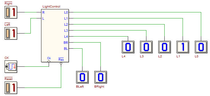
In this lab we will design, as a Finite State Machine, a simple Light Controller. After verification with the simulation, we will implement a physical prototype on FPGA and test it. The system architecture is show in the figure below: The system is composed by a synchronous FSM with two input !Right e !Left, active low, corresponding to two push-buttons on the board; five outputs L4-L0, connected to the lights; two control outputs BLeft e BRight. At the reset, the FSM activates L0. Pressure and release of !Left switches off the light that is active and switches on the one on the immediate left. The same action, pressure and release of !Right, switches off the light that is active and on the one on the immediate right. When the light is in the leftmost position (L4) the system accepts only the !Right command, when it is in the rightmost position (L0), only the !Left. One light only can be on at all times. The output BLeft signals that the corresponding button !Left is pressed; BRight signals that the corresponding button !Right is pressed. A trace of the ASM chart is available here. State variables X,Y, Z, W, outputs L4, L3, L2, L1, L0, BL (BLeft), BR (BRight), inputs L (!Left) and R (!Right) are already defined. In the trace, five state blocks (a4, a3, a2, a1, a0) are already present. They correspond to the states where one of the output lines L4, L3, L2, L1, L0 is activated and the system waits for the buttons input. A hint on the logic of state a2 is provided. After the design of the ASM chart, you should verify, using the timing simulation of the d-FsM, that the functionality of the FSM corresponds to specifications. The FSM should then be imported as a component on the d-DcS. It is certainly useful to repeat system simulation on the d-DcS, both in animation and timing modes. To that purpose a schematic to be completed is available here, in which to insert the FSM. We recommend to use the schematic supplied, without modifying the input and output terminations, since they contain the information needed for exporting the project on the FPGA board. At this point we begin the procedure for the physical implementation of the project in the FPGA board. The general procedure is described in the introductory tutorials:
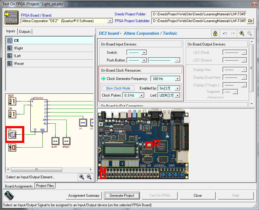
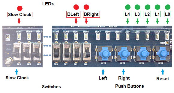
The command "Test on FPGA" opens the dialog window shown below: All the needed associations between d-DcS schematic and the FPGA board input/outputs are already set in the given schematic: it is not necessary to modify them. The clock CK is set to 100 Hz, a frequency rather low but adequate for the human interaction with the system. The "Slow Clock Mode" has also been set: as configured in the figure above, this mode is activable at run time using switch SW[17]. The "Slow Clock" is set to the frequency of 0.5 Hz, and it is displayed by the red LED LEDR[17]. According to this setting, if the switch is set to zero, the clock CK will work at the "normal" frequency of 100 Hz; if the switch is set to one, the clock frequency will be reduced to 0.5 Hz. In this mode, the network functionality can be tested with a simple visual observation. Note that the clock programmability feature is not a particularity of the FPGA board, but it is obtained by the design exportation process. This process adds a network to the project, based on counters, that "scales down" the on board 50 MHz clock to the desired low frequency. For the convenience of the experimenter, the associations are highlighted also in the next figure, that can be considered as a "control panel", useful for testing the physical system: Using the switches and buttons shown above, and observing the status of the LEDs, it is now possible to test the system. | |||||||||||


