|
|
||||||||||
|
In this laboratory you are asked to complete the design of an asynchronous serial communication system based on microcomputer. After the simulation of the project, you'll realize a prototype on FPGA to verify the actual operations. The system architecture is shown in figure:
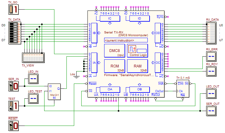
The system is composed of two The following figure shows the schematic of each microcomputer:
In the figure, from above and from the left, are visible:
Nella figura è visibile inoltre, sulla destra in basso, la presenza di un componente Interrupt Timer, predisposto per interrompere ciclicamente il microprocessore ogni 0,1 mS. In the figure is visible also, on the bottom right, an Interrupt Timer component, arranged for interrupting the microprocessor cyclically every 0.1 mS. Transmitter module TX specifications
The Bit Time is equal to 1.6 mS, equal to 16 times the time interval marked by the Interrupt Timer component. The control signal TX_GO has a minimum duration of 2 mS (the maximum is not specified). Receiver module RX specifications The receiver RX waits for serial packets on line SER_IN (it is assumed that the TEST input is '0'). When the start of a packet is identified (the start bit = '1'), the receiver synchronizes the data acquisition and, in order, extracts the eight bits of information from the packet and makes them available, in parallel, on the outputs U0..U7 (via the port OD). Finally, if the Stop Bit is received correctly = '0', the receiver activates the output RX_RDY for a time equal to 1.6 mS; otherwise, if the Stop Bit is '1', the receiver activates RX_ERR until SER_IN returns to '0'. The input TEST allows to choose the source of the serial sequence to decode. If TEST is activated, the sequence comes from the serial line SER_OUT of its own transmitter. In this mode, we can verify the functionality of the system of transmission/reception on-site, without the need to connect it to a second system.
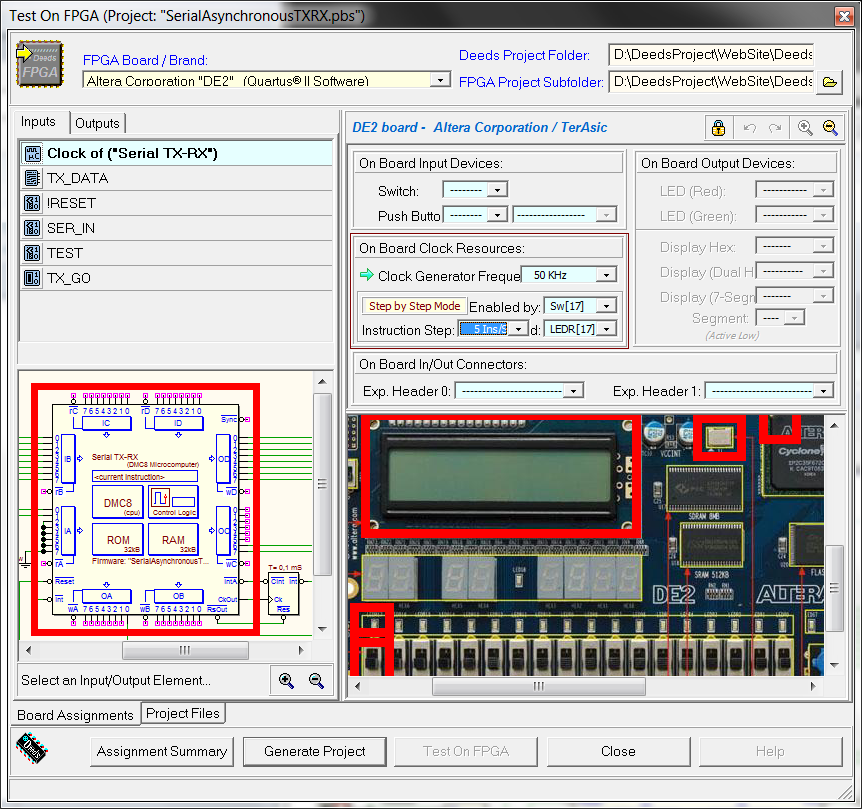
Who wants to deal only with the analysis of already written code, and the simulation of the system, will find here a complete solution. At the end of the writing and the functional test of the program (in the d-McE), you must program the microcomputer ROM (you can open the schematic in the d-DcS by clicking here). In the d-DcS timing diagram window is available an appropriate test sequence. It is recommended to use the provided schematic without to delete or change the input and output terminations, because they have been set for the export of the project on the FPGA board. At this point we begin the procedure for the physical implementation of the project in the FPGA board. The general procedure is described in the introductory tutorials: The "Test on FPGA" command of the d-DcS will open the following dialog window:
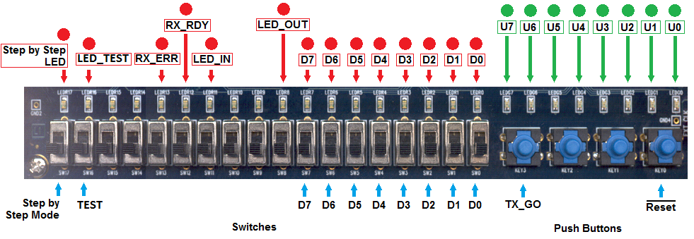
Note that all the needed associations between d-DcS schematic and the FPGA board input/outputs are already set in the given schematic: it is not necessary to modify them. The clock of the microcomputer, as you can see in the figure, is pre-set to 50 KHz (a frequency sufficiently low to allow a visual control of the the serialization and de-serialization of the bits). Nothing prevents to set, in a second moment, the clock frequency to the nominal value (10 MHz). The “Step by Step Mode” has been enabled, assigning to the switch Sw[17] the task to activate it at runtime. This means that if this switch is set to zero (lever toward us), the clock CK works normally at 50 KHz, but if it is set to one (lever in the other direction), a debugger circuit is activated to slow instructions execution, for diagnostic purposes. LEDR[17] has been selected to visualize the clock pulses being sent to the microcomputer (a execution frequency of 5 instruction per second was chosen). All defined associations are highlighted also in the next figure, useful for testing the physical system:
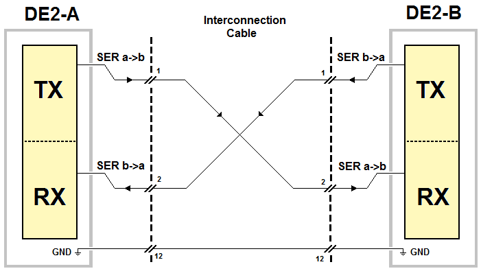
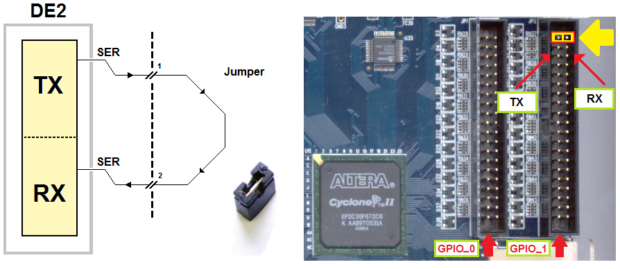
We can test the system stand-alone by activating the test mode (switch TEST upward), or by using two separate boards, interconnected by means of an appropriate cable, to exchange data in both directions: We make the connection using one of the two 40-pin connectors available on each FPGA board. As seen in the figure above, we use a cross-connection between the transmitter and the receiver, in both directions, for a total of 3 wires (including the ground reference GND). Here the pattern of the connection schematic, which refers to the expansion connector "GPIO_1" present on the board. Even without activate the TEST switch, we can perform preliminary tests with a single board, using a simple jumper inserted into the connector, as shown in the following figure (yellow arrow), in order to connect with the transmitter and receiver: Be extremely careful in placing and removing the bridge, to avoid mechanical damage to the connector pins. To avoid possible damage to the FPGA chip, whose pins are directly connected to the connector, it is necessary to carry out this operation when power is off. | |||||||||||


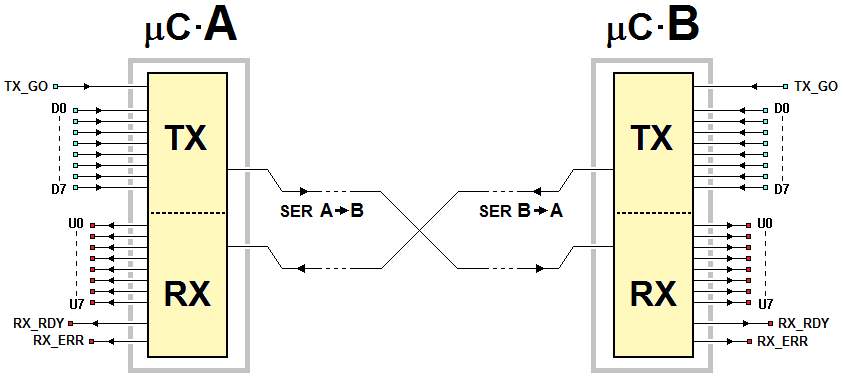
 and
and  identical microcomputers, interconnected between each other through two lines. Each microcomputer includes software modules that realize, with interrupt techniques, a transmitter (TX) and a receiver (RX) of the serial line. The microcomputer working with clock at the same frequency (10 MHz), but independent between them. Let us now examine the design specifications of the modules TX and RX.