|
|
||||||||||
|
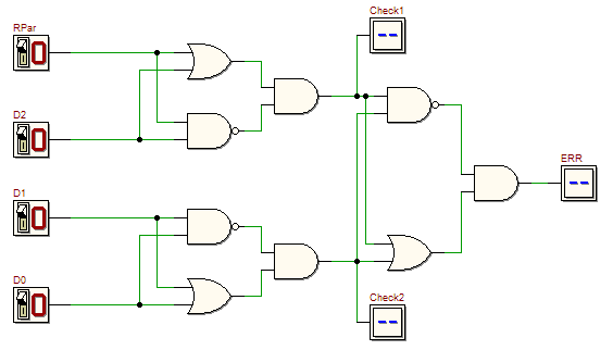
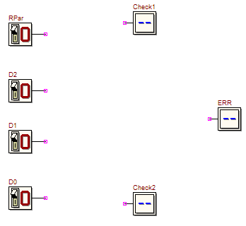
Click on the figure to open the schematic below in the d-DcS: Using the simulation by animation, compile a truth table describing its behaviour. Write the boolean expression of the outputs Check1, Check2 and ERR, resulting from the schematic (not the truth table). ERR can be written using Check1, Check2 as inputs. Next, from the truth table, observe that it is possible to perform the same function using only three EXOR gates. Write the new expression of ERR in terms of EXOR gates (use the notation “x EXOR y” or “x XOR y”), and draw the new schematic, using the following one to be completed (click on the figure to open it in the d-DcS): First, check the correctness of your design using the functional simulation. This circuit can be used to verify if the Parity of the data D2, D1 and D0, which is represented by the bit RPar (= Received Parity), has the same value as the Parity calculated by this network. The output ERR is activated when RPar and the re-calculated Parity do not match. It can be useful to simulate the net with the timing simulator: we suggest to use the two test sequences shown below (available in the Timing Diagram window). The first test sequence demonstrates a correct sequence of received data:
The second test sequence shows a received data containing errors, due to noise or electrical problems in the system that carries the four bits. We assume that, as highlight in red, two bits have been altered: D1 on the second set of values, and RPar on the fifth set.
|
|||||||||||


