|
|
||||||||||||||||||||||||||||||||||||||||||||||||||||||||||
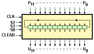
In this laboratory you are requested to write a DMC8 assembly program that emulates a 12-bits Register/Counter (see the figure below) and to test its functionality, not only by simulation, but also prototyping it on a FPGA board.
This particular 12-bits Register/Counter has the following input/output terminations:
When the synchronous CLEAR is active, on the next CLK positive-edge the device outputs are cleared. When CLEAR is not active, the device, accordingly to the function set by S2, S1 and S0, will act as a parallel register, or a rotating shift register, or a cyclic up/down counter. When the requested function changes, the component retains the data value on its outputs (remember that the real component is made of flip-flops). The following table details the modes of operation:
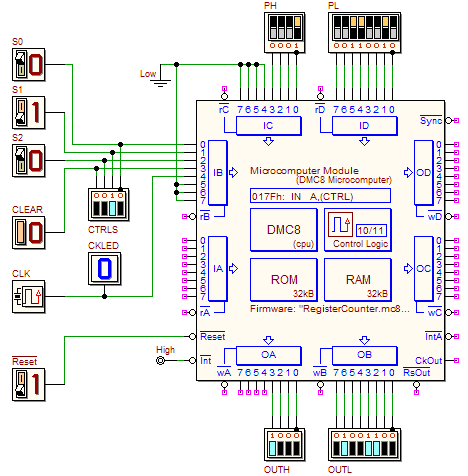
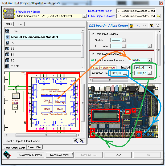
To emulate the device, we configure a microcomputer system, as shown in the following schematic (just click on the figure to open it in the d-DcS): We use three parallel input ports (IB, IC and ID) and two parallel output ports (OA and OB). The lines CLK, CLEAR, S2, S1 and S0 are connected, respectively, to the bits 4, 3, 2, 1 and 0 of the IB input port; P11..P0 to IC and ID input ports, and U11..U0 to OA and OB output ports. The program starts on the activation of the system hardware RESET. Two different traces of the code, to be completed in the d-McE, are available here: the first one is more challenging; the second one contains more suggestions. When the program is completed, perform a preliminary test of its functionality in the d-McE debugger. At this point, load the program in the microcomputer ROM, and simulate the system with the timing simulator At this point we begin the procedure for the physical implementation of the project in the FPGA board. The general procedure is described in the introductory tutorials: The "Test on FPGA" command of the d-DcS will open the following dialog window:
Note that all the needed associations between d-DcS schematic and the FPGA board input/outputs are already set in the given schematic: it is not necessary to modify them. The clock frequency is set to 10 MHz. The “Step by Step Mode” has been enabled, assigning to the switch Sw[17] the task to activate it at runtime. LEDR[17] has been selected to visualize the clock pulses being sent to the microcomputer. Pushbutton Key[03] has been chosen to control the manual execution of the instructions. If Sw[17] is at '0', the debug system is not active and the microcomputer works with the "normal" clock (10 MHz). If Sw[17] is turned on at '1', the system stops clock generation and the debugger waits for the user to press Key[03] (each activation of the push-button executes one instruction). All defined associations are highlighted also in the next figure, useful for testing the physical system:
| |||||||||||||||||||||||||||||||||||||||||||||||||||||||||||


 of d-DcS (a proper test sequence is available in the timing simulation window). We recommend to avoid any change of the input/output terminations, that have been setup for the next step: exporting the project on the FPGA board.

