A system based on the DMC8 microprocessor
2.1 The DMC8 microprocessor
2.1.9 An initial example of programming

2.3 Input/output and memory subsystems
2.3.1 Memory subsystems
Example of Read-only Memory (ROM) system.
The simulation can be performed 'by animation', paying attention to the address provided to the memories, which must be between 0000h and 1FFFh. By activating both !MEMREQ and !READ to zero, the reading of the ROM locations will be obtained on the data bus (only the first 4 locations of each device have been programmed for test purposes).

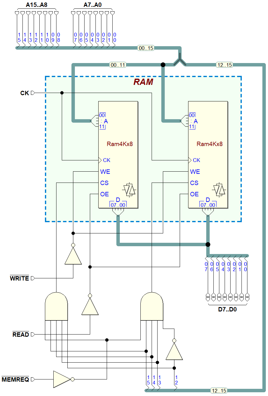
Example of Memory Write/Read (RAM) system.
This is the figure reported in the book (pay attention to the note below the figure):
However, to simulate the network it is necessary to add a tri-state buffer which allows us to supply the data to be written on the bus. By clicking on the next figure, the network set up for simulation will open in the Deeds-DcS.

The simulation can be performed in animation, paying attention to the address provided to the memories, which must be between E000h and FFFFh.
Before writing anything significant in the RAM, the locations will contain random values. Therefore, from the point of view of the simulator, indeterminate. By activating both !MEMREQ and !READ (bringing them to zero), unknown values will be obtained on the data bus, whatever is the supplied internal RAM address.
To write data:
- Set the value of the data at the input of the tri-state buffer connected to the switches named WRITE DATA;
- Define the address of the location you want to write;
- Activate (at zero) the memory request !MEMREQ;
- Activate (at zero) the write command !WRITE and wait for the next rising edge of the clock;
- Deactivate !MEMREQ and !WRITE.
To verify the successful writing, you need to:
- Keep fixed the address of the location you want to read the same as before;
- Activate the memory request again !MEMREQ;
- Set the !READ command to zero, waiting for the next rising edge of the clock;
- The data will appear on the bus, ready to be used;
- To complete the reading, you must then deactivate !MEMREQ and !READ.
2.3.2 The Input/Output subsystem
2.3.2.1 Parallel output ports
Example of parallel output port, with address definable by means of switches. The simulation can be performed 'by animation'.
To write data to the output port:
- Provide the port address (25h in this example);
- Set a value on the data bus;
- Activate (at zero) the input/output request !IOREQ;
- Activate (at zero) the write command !WRITE and wait for the next rising edge of the clock;
- Deactivate !IOREQ and !WRITE.
The data will remain stored in the register until the next writing. Please note that the port cannot be read (there are no circuits for reading it).

2.3.2.2 Parallel input ports
Example of parallel input port, with address to be set with switches. The simulation can be performed 'by animation'. The 'outside world' is supposed to provide us with the data to be acquired, via the INPUT DATA lines.
- With the address bus we generate the address of the port to be read (set on the switches at 83h, in this example);
- We activate (at zero) the input/output request !IOREQ;
- We activate (at zero) the read command !READ, so the tri-state buffer will show the data on the bus, ready to be read by the processor;
- We deactivate !IOREQ and !READ, disengaging the bus.

2.5 Exercises
2.5.1 Memory systems
By clicking on the next figures, the networks set up for the simulation will open in the Deeds-DcS. A tri-state buffer has been added to the networks, to allow the data to be written to be supplied on the bus.
Exercise 2 (schematic to analyze):

Exercise 3 (schematic to analyze):

Exercise 4 (schematic to complete):

2.5.2 Parallel input/output ports
By clicking on the next figures, the networks set up for the simulation will open in the Deeds-DcS. A tri-state buffer has been added to the networks, when necessary, to allow the data to be copied to the port to be supplied on the bus.
Exercise 1a (schematic to analyze):

Exercise 1b (schematic to analyze):

Exercise 1c (schematic to analyze):

Exercise 2 (schematic to complete):

2.6 Solutions
2.6.1 Memory systems
Solution of exercise 4:
By clicking on the figure, the network, set up for simulation, will open in the Deeds-DcS. A tri-state buffer has been added to allow the data to be written to RAM to be supplied on the bus.

2.6.2 Parallel input/output ports
Solution of exercise 2:

2. Errata Corrige (Chapter 2)
None