Version Notes
(Ver. 1.95.500 - Jan 2, 2016)
 Deeds-DcS (Component Library, Schematic Editor)
 The addition of new components has produced a change in the internal version of the Deeds-DcS (.pbs) file format (now: 1.028). As usual, old files are readable by the new version, while files created by the current version are not compatible with the older ones.
Starting with the present release, the Input and Output components and, in general, the other ones having an user-definable label, appear with a default label (light-blue colored and between brackets, showing the internal numerical identifier), immediately after being inserted in the schematic:
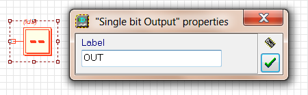
The default label represents a placeholder, and suggests to the user that such components may be named. In the example of the next figure, the user has opened the Properties Dialog of the component (to assign the name 'OUT'), with double-click on it.
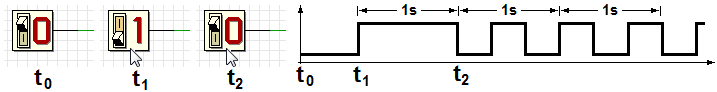
We added, in Animation mode simulation, the ability to produce automatic repetition by the input components "Clock Generator", "Input Switch", and "Input Dip-Switches". If, after a click on the component, the user holds down the mouse button (instead of releasing it), after a short latency time, the input component starts to toggle its value. The value changes at slow speed, in order to permit the observation of the circuit behavior. This feature is not active on push-buttons, given their particular functionality; also, it's not active also on the DMC8 component clock, where it would be impractical. Obviously, the repetition feature on Clock components is inhibited when they are animated.
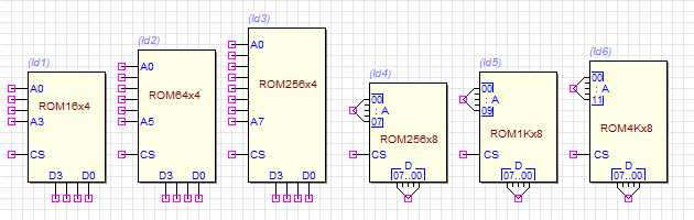
Two ROM types have been added to the library, the sizes 1K x 8 and 4K x 8: now, the available ROM are:
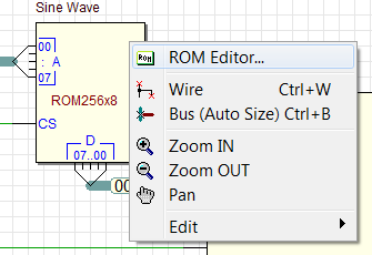
Moreover, now the contents of a ROM are editable in a few new modes, included the possibility of initialize the memory with a sampled waveform. In the example of the next figure, the user has activated the contest menu of the component, to launch the ROM Editor/Programmer:
The ROM Editor/Programmer dialog (see the figure below), has been enhanced with the addition of three new buttons ("Load", "Save", "Waveform"), and the Label field. As in the previous version, the dialog allows to edit the ROM contents in manual mode (Undo/Redo buttons available): the supported formats are: hexadecimal, binary and ASCII text.
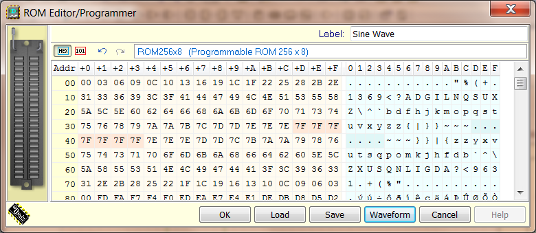
In the new Label edit field (up-right side), the user can edit a descriptive name for the memory component (see also the example in the previous figure, just over the symbol: "Sine Wave").
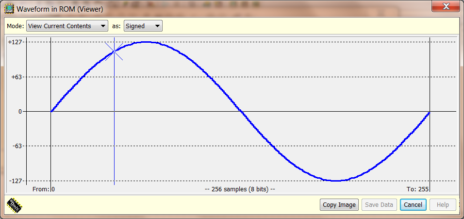
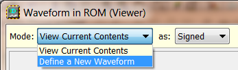
By clicking on the Waveform button, we open the"Waveform in ROM" dialog, initially in the Viewer Mode. As visible in the next figure, the dialog shows the Rom data as a digital signal, in a bidimensional chart (on the horizontal axis: the internal addresses of the memory; on the vertical axis: the corresponding data values). In this example, the memory contains the 8-bits samples of a complete cycle of a sine wave (the samples are coded as signed binary numbers).
To define a new waveform, you must change the
mode (see the figure below):
Now it is possible to choose a new waveform, selecting it from the Wave list box:
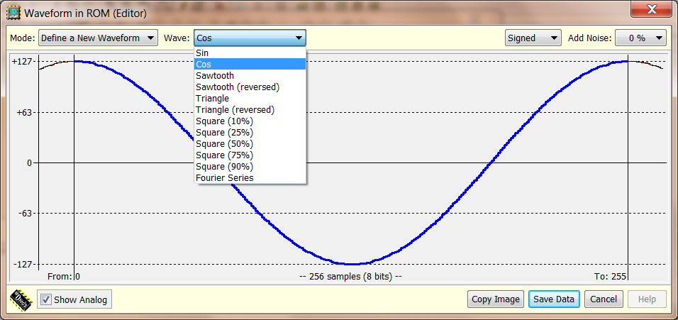
The user can select a standard function: sine, cosine, saw-tooth, triangle and square wave (in the figure above, the cosine waveform). The waveform samples are calculated to memorize an entire cycle of the wave and to reach the maximum possible amplitude, centered on the zero (from +127 to -127, if signed, as in this example), or all-positive ( unsigned, from 0 to 254).
The button "Copy Image" will copy the waveform image on the clipboard, ready to be pasted in the user documents.
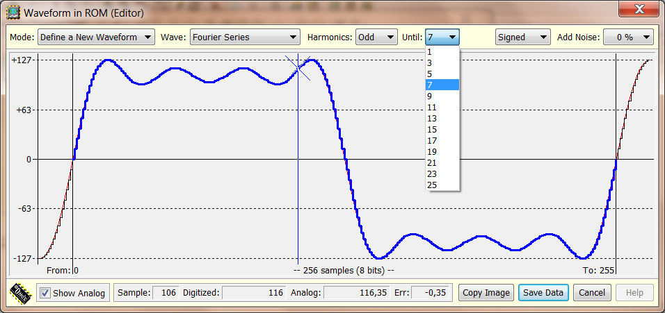
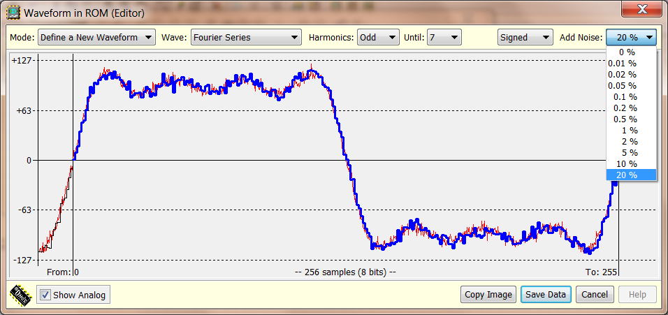
At the end of the list, a Fourier Series utility is available (the Fourier Series is a mathematical method to represent a cyclic function as the sum of sine waves). We can choose between two classic series (square wave and saw-tooth wave), and stop the series at a given order. In the example below, a square wave series is set (as only the "Odd" harmonics has been selected), limited at the seventh harmonic.
Moving the mouse on the desired sample, with a click, the user will open a magnifying window (visible in the next figure):
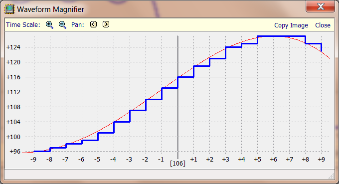
In this example, we see a particular of the waveform seen in the previous figure, magnified around the sample of address 106, whose value is +116 (in blue, the digitized waveform; in red, the analog original waveform that has been sampled).
Buttons are available to manage time scale and horizontal Panning; the vertical scale, instead, is adaptive. Also here, a "Copy Image" button allows to the user to copy the waveform image on the clipboard.
Returning to the Waveform Editor, note that we can add to
the waveform also a certain amount of white noise, as visible in the following figure:
Let's return to the ROM Editor/Programmer dialog, and consider the buttons "Load" and "Save":

The ROM memory contents can be saved on, and loaded from, a coded text file. The default extension of the file is ".drs" (Deeds Rom Source file), but it can be opened and modified with a text file editor. By clicking on the "Save" button, we export a text file like this:
#- Deeds (Digital Electronics Education and Design Suite)
#- Rom Contents Saved on (14/10/2015, 19:03:29)
#- by the Deeds (Digital Circuit Simulator)(Deeds-DcS)
#- … omissis …
#-----------------------------------------------------------
#R ROM256x8, id 02F0
#A 0000h
#H ;
4E 65 6C 20 6D 65 7A 7A 6F 20 64 65 6C 20 63 61
6D 6D 69 6E 20 64 69 20 6E 6F 73 74 72 61 20 76
69 74 61 20 6D 69 20 72 69 74 72 6F 76 61 69 20
… omissis …
In this example, the #- in first position indicate that the entire line is a Comment. A # followed by a letter is a Directive (see below). All the HEX numbers that will follow, in the lines without # in first position, represent the data contents of the ROM, location by location.
By clicking on the "Load" button, we can import a .drs file. The file is compiled and the ROM component is programmed with the file data. A Directive must be written in first position, and can be one of the following:
#R ROM256x16, id 0004 Rom component Type (ignored at compile time);
#A <address> Start address of data that will follow (hex or decimal),
if no #A directive is defined, the default address is zero;
#T "Text contents follow", that is read starting from the next
line (including CR/LF), and stored from the address defined
[this is the default];
#H Declares that the following numbers are hex;
#B Declares that the following numbers are binary;
#D Declares that the following numbers are decimal.
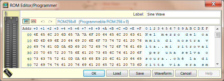
In the following example, the file has been coded to load in the memory the first verses of the "Divina Commedia" (Dante Alighieri). Note that the directives could be cut away, leaving only the text in the file:
#- Dante Alighieri
#-----------------------------------------------------------
#A 0000h
#T
Nel mezzo del cammin di nostra vita
mi ritrovai per una selva oscura
ché la diritta via era smarrita.
Ahi quanto a dir qual era è cosa dura
esta selva selvaggia e aspra e forte
che nel pensier rinova la paura!
Then, the resulting contents will be visible in the ROM Editor/Programmer (see the next figure):
A new component type has been added to the library: the Digital to Analog Converter (DAC). In the following figure, the menu shows the available bit-sizes (4 and 8 bits):
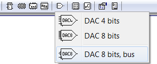
When inserted in the schematic, the three DACs are represented by the symbols:
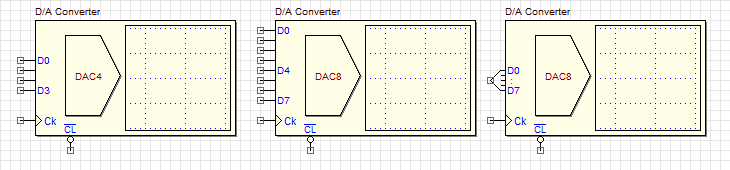
The converter functionality is symbolized by the pentagone on the left side; on the right side we see a square empty area. During thesimulation, in this area the converted values are plotted by a pen, forming a chart logging the generated waveform. These DACs are intended for displaying digital signal generation: they accept signed numbers (see the figure below).
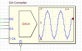
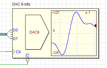
At the input, the DAC behaves as a parallel register, and as a output data display device by the other side. Note that no analog output is really generated.
On the positive edge of the clock (Ck), the data is loaded in the DAC register and then added to the display chart. When the clear input (!CL) is activated, the DAC register is reset, and also the output chart is cleared.
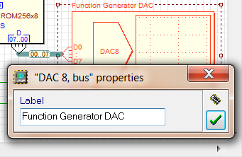
In the figure below, the user has double-clicked on theDAC component, opening the Properties Dialog to assign to it a specific label (in this example: "Function Generator DAC"):
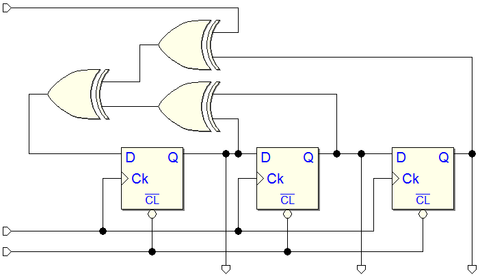
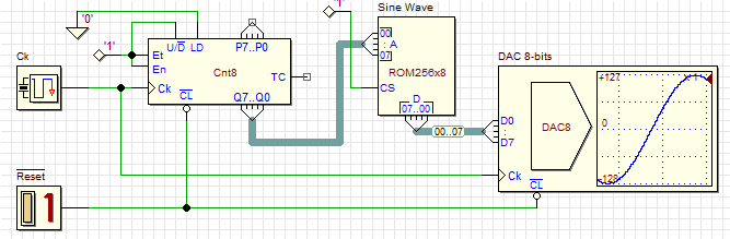
The circuit in the next figure, available in the demos, shows a simple use of a 8-bits DAC. The 8-bits counter generates cyclically all the addresses of the ROM (256 cells, 8 bits each). The ROM contains the 256 samples of an entire cycle of a sine will generate a sine wave having frequency F = Fck / 256.
The Baloon Hints has been eliminated because too
invasive, returning to the previous simple standard Hints. For instance, if the mouse moves over thememory component button, now you see the related hint "Memories" (near the button), and a more complete description on the Status Bar (at the bottom of the window):
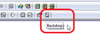
Introduced a new component: the "Backdrop". A Backdrop permits to highlight part of the schematic, putting in evidence, for instance, its function. In the next figure a few examples of the offered possibilities:
Note that the Backdrop is not a "container", as it would seem, but only a sort of a decoration, and it stays always in background. The command to insert a Backdrop is on the Component Toolbar:
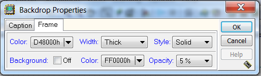
Immediately after the insertion of a Backdrop (that acquires a default size), the Backdrop Properties dialog is shown automatically:
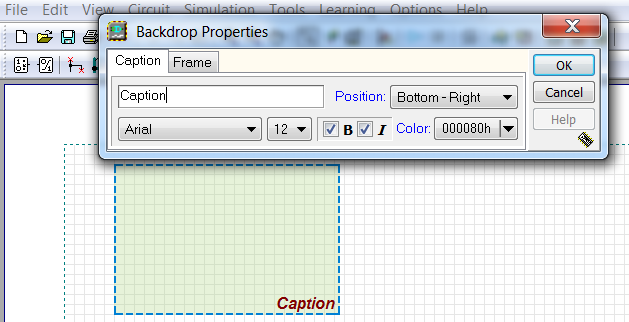
A change in the parameters will modify immediately the aspect of theBackdrop. In the dialog page Caption, the user can define a short caption, its position, color and font properties.
In the page Frame, instead, background and border properties are definable (see the next figure). Note that it is possible to define also the Opacity of the background color:
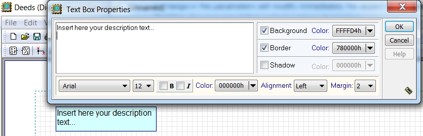
In this version, we have revised the Text Box Properties dialog (see the next figure). As for the Backdrop, a change in the parameters will modify immediately the aspect of the Text Box.
The user can define the text, its position, color and font properties, as well background and border properties. Moreover, now it is possible to set a very small font size (5, 6, 7, 8 and 9 point; before, 10 was the minimum).
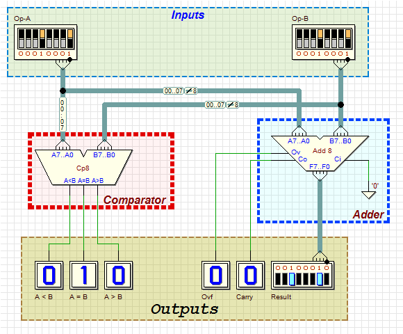
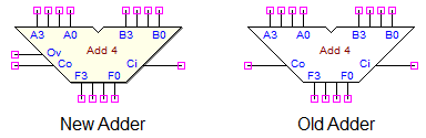
We have modified all the Adders in the library, because they did not have the Overflow output (for signed numbers). For compatibility reasons, the adders (4 and 8 bit) previously released with version 1.92.200, have been moved to the obsolete library (accessible via the menu "Circuit"). Any circuit employing the old adders will continue to operate; if you want to replace them with the new ones, they are pin-compatible, except for the added pin "Ov".
We added to the library a new component, the"Complementer", in the 4 and 8 bits sizes:
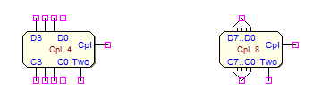
These components have two control inputs, Cpl (Complement) and Two (Two's or Ones complement):
Cpl |
Two |
function |
'0' |
'x' |
Output = Input (as is) |
'1' |
'0' |
Output = Ones' Complement of Input |
'1' |
'1' |
Output = Two's Complement of Input |
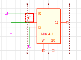
Now the Error Checker highlights, in the editor, the input pin that is not connected, displaying a little red square around it (previously, the entire component was highlighted).
In this version, when inserting a new component, its "orientation" is always the default (right). This change simplifies the addition of a new component; in the previous versions, the command maintained the orientation previously defined.
The functionality of the right mouse button, regarding the insertion of wires and buses, has been changed: if the right mouse button is pressed for a long time (at least half a second), we exit the insertion command (as in the case of insertion and pasting of components). If the right mouse button is released before that time, we return to the possibility of starting a new piece of wire or bus.
Now the edit command "Copy Image" saves the image of the circuit together with the drawing grid, if this is currently displayed in the editor. In addition, now the generated image is aligned with the grid and properly limited to the edge of the design.
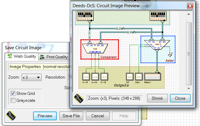
Similarly, the "Save Circuit Image" dialog includes the design grid in the image, if the new control "[x] Show Grid" is set (see the figure below). Also in this case, the generated image is aligned with the grid and properly limited to the edge of the design. Starting with the current version, the " Save Circuit Image" dialog always saves the current setting, not only when closed with the OK button.
Now, in the "Save Circuit Image" dialog, the preview window is no longer a modal dialog: it may be placed alongside the dialog itself. By changing the setting parameters, the preview window is updated immediately.
Introduced a new component, a simple Un-decoded Seven Segments Display (in the next figure). This display accompanies those already included in the library, that are decoded. Like the others displays, it take place in the
timing diagram, with an expandable track, and can be exported in VHDL, for testing on FPGA.
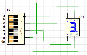
In the timing diagram, its sub-tracks are named according to the standard name of the segment (a), (b), (c), (d), (e), (f), (g) and (dp), where dp = Dot-Point.
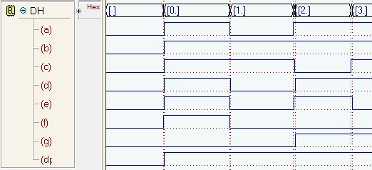
Since the segments and the dot-point are driven by separate wires, the presence of one or more "unknown" values is handled line by line. If a line is driving an "unknown", the segment appears simply colored differently (as shown in the figure below, on the left side).
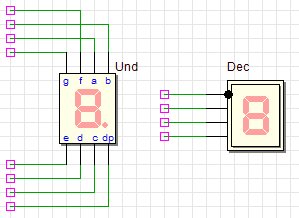
Consequently, we eliminated the representation of the letter "U" ("unknown") in all the other display components, for consistency. For example (on the right side of the figure), in case of unknown, an"HEX coded" display will showall segments undefined, and no longer the "U".
Fixed a bug related to the simulation by Animation: the mouse wheel not only controlled the drawing scale but, at the same time, also the position of the clock speed cursor. Now, the mouse wheel does not act anymore on the clock speed cursor position.
Fixed a bug related to the internal "netlist" connection of the Bus Multiplexer pins.
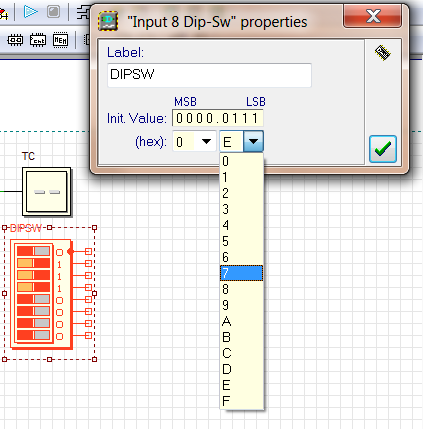
In the Properties Dialog of the array type input components (such as Input Dip-Switches, 4 and 8-bits), we updated the functionality of the Hex/Bin value editor. Now, while choosing the Hex value in the list box, the corresponding binary value will be shown, in real time, in the upper field (see the next figure):
Fixed a bug about the "Source Code" window of theDMC8 Debugger: now the display of the source code is "read-only", as it should be.
Fixed a bug about component move. Previously, when moving a part of the circuit, a shadow of the component (label and pin names) remained temporarily on the screen; moreover, the background grid was not correctly redrawn. Now, with the revision of the graphics due to the introduction of the new "Backdrops", this bug has been corrected.
Deeds-DcS (FPGA Extension)
The support for available FPGA boards has been extended. Now it is possible to create projects for the following educational boards of the Altera® Corporation (using Quartus® II Software, web-edition):
"DE1", "DE2", "DE2 - 70",
"DE2 - 115".
Special thanks to Marcelo Dantas that suggested and helped us to support the "DE2-70" board. He filled most of the (tedious) board-specific tables, and he executed testing on this and a few other boards. Note that on the "DE2-70", the " dot point" of the seven-segment displays are connected to the FPGA chip, while on the "DE1", "DE2" and "DE-115" they are un-connected. So, support for editing the dot point connection has been added to the "Test on FPGA" dialog.
This suggestion came first from Marcelo Dantas, but also
from colleagues as Davide Anguita and Luca Oneto, that started to use more than one type of board: when users need to work on more than one type of FPGA Board, maybe they can't use the same version of FPGA software for all.
For instance, the Altera DE2 board is supported by Quartus-II v.13, but not by Quartus-II v.15: so, users needed to install both the Quartus-II versions.
Now, in the dialog that allows to launch the FPGA tool (after the VHDL generation), the user can select which executable will be launched, for each specific FPGA board (see figure below), by clicking the "Configure" button:
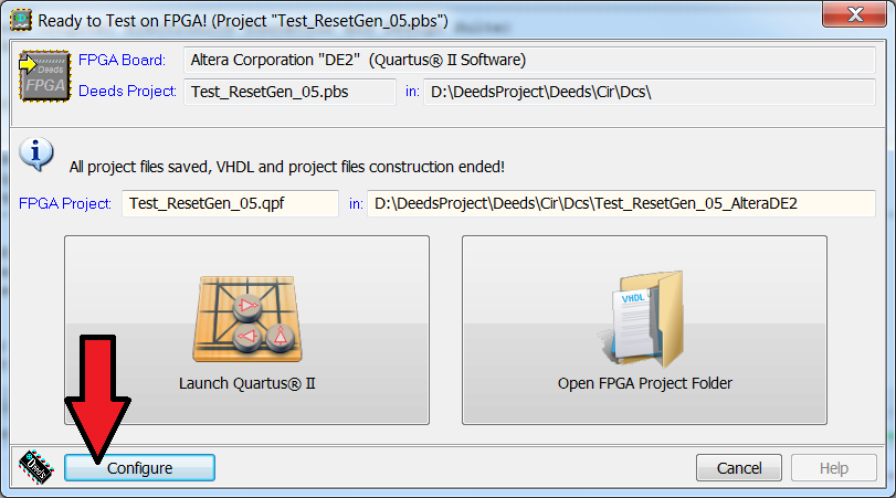
Once this button is pressed, the bottom of the dialog changes as in the following figure:

The user can: a) keep the previous default, as in the older Deeds versions (leaving the operating system to launch the tool registered for a given project file extension), or b) select the correct executable to be launched (for the board in use in the current project).
The button "Save Configuration" permit to save the setting, hiding these configuration fields.
Regarding the conversion in VHDL code and the generation of the FPGA Project Files, we added protection on the names given to VHDL files and VHDL Entities, to be all VHDL compliant, regardless of the original file names (file names could be modified by the download operation in the web browser, or by a voluntary re-naming). Starting from the present version, the user is no longer required to manage "a priori" VHDL compliant project file names because conversion will consider this issue, changing "a posteriori" all the not compliant names.
Now, in the "Test on FPGA" window, the VHDL subdirectory is created only when the user starts the VHDL generation. Previously, it was created immediately, on the opening of the window. Before generating the VHDL, or when selecting a new FPGA board, the subdirectory name is only suggested to the user. Consequently, the button that opens the sub-directory, in the top right of the window, is enabled only if the directory already exists or after the VHDL project is generated.
Fixed a bug: in the text headers of the generated VHDL files, the name of the FPGA board in use and the FPGA chip name remained the same even if we choose a different board in the export settings.
The following bugs, occurring in the "Test on FPGA" window, has been fixed:
a)
When deleting an association between an input/output component and a device
on the FPGA board, the database was "silently" altered, so that an error
occurred just on re-opening the "Test on FPGA" dialog again.
b)
When we set a clock, without defining together also the "Slow Clock Mode",
an error occurred when generating the VHDL code.
c)
It was impossible to delete a previous association between an input
component and a board switch, when a scaled frequency clock was defined
without setting the "Slow Clock Mode".
d)
A similar issue regarded the on-board red LED's, and the HEX displays
(single and dual).
Note that this version of Deeds doesn't
support VHDL generation of the Digital to Analog Converter components.
Deeds-DcS (Timing Diagram)
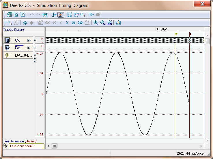
The Timing Diagram Window has been enhanced with new features. The most evident is the support for the Digital to Analog Converters (described in the previous section "Component library, Schematic editor"): we can display the DAC output signal, in a quasi-analog representation.
In the next figure, we see the timing simulation results of a circuit including a DAC:
Note that the Magnifier can enlarge horizontally a part of the display also if it includes these kind of tracks, as visible below:
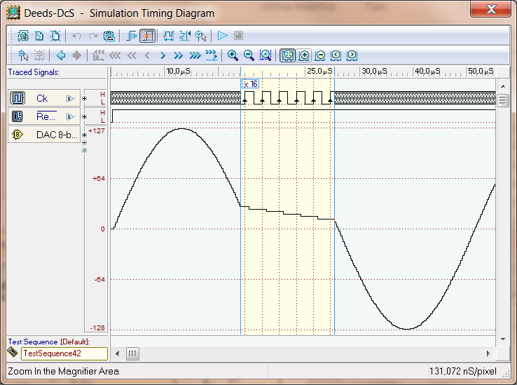
Moreover, to make readable the amplitude values of the digital signal, now the vertical axis is completed with a few reference values (+127 ,+64, 0, -64,-128, in the example above). Also the vertical scale of the tracks has been enhanced: now it can be zoomed until a x 32 factor.
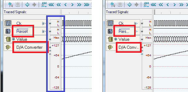
We changed the graphic aspect of track labels andbuttons, because with the introduction of theDAC components was also necessary displaying some additional information (see the figure below, highlighted in blue). Moreover, now the track names are shortened according to the available space (here, highlighted in red):
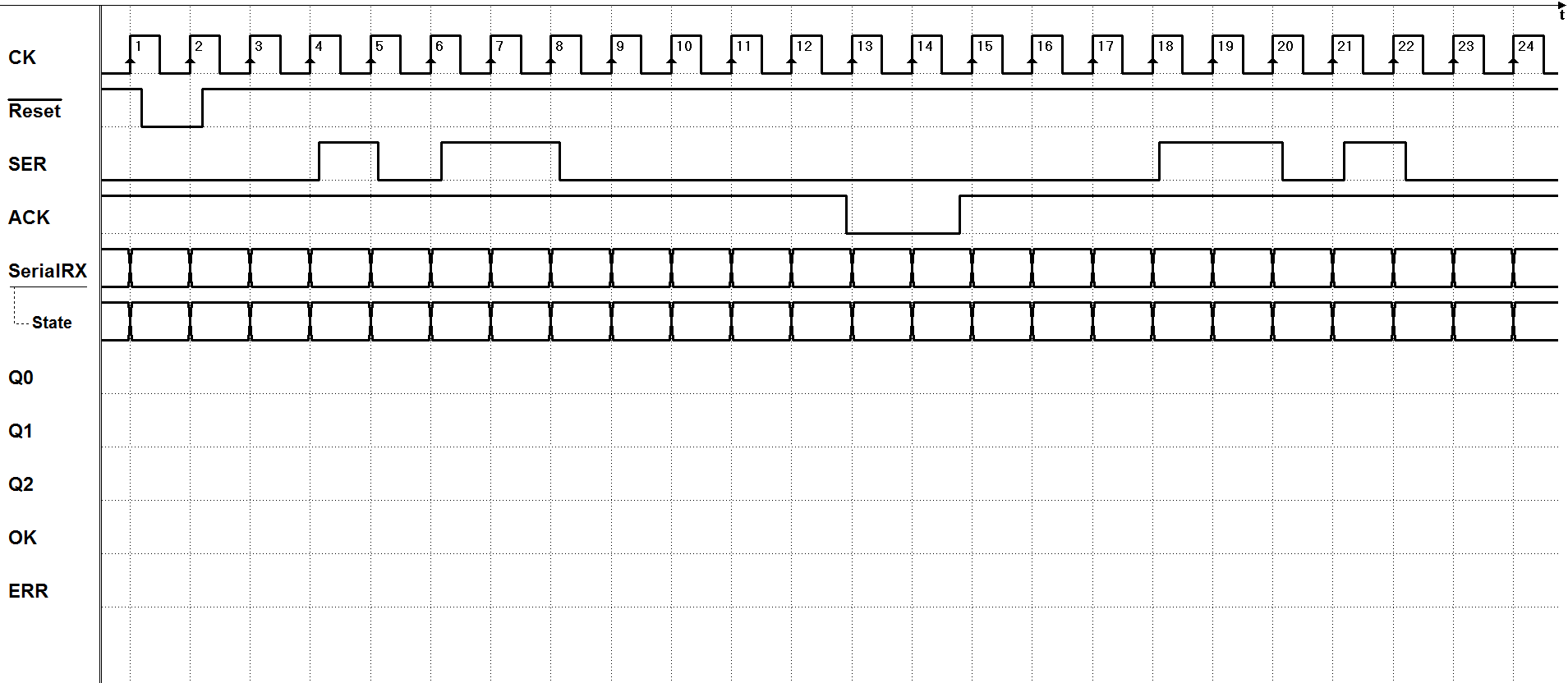
A new feature of Timing Diagram Window is the automatic assignment of the Time References (as visible in the next figure, the Time References are represented as dotted vertical lines). These lines allow to relate all the logic values changes with the time events of a particular track, for instance, a clock track):
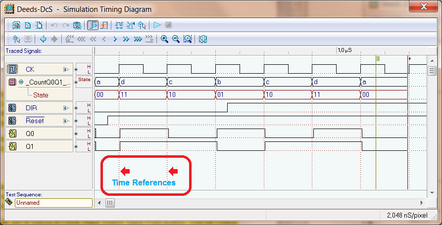
Now, when we open the Timing Diagram Window, the "Time References" are automatically assigned, as a first choice, to the higher track, if this is a clock. If we haven't a clock track, it is assigned to a micro-computer track; in the lack of clocks and micro-computers, it is assigned to the first track, of whatever kind it is.
We have introduced signal edges highlighting, that could
be activated, or not, for the track that defines the "Time References" (described in the previous paragraph).
The highlighting is possible for the tracks of type Clock,Input Switch, Input Push-Button, Simple Output:
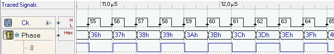
The highlighting consists in (see the figure above):
a) numbering of edges (corresponding to the Time References), for documentation purposes;
b) marking of edges with an little arrow, up or down (only for Clock tracks).
Numbering and marking can be hidden (always together) and follow the user's choices about the Time References: 1) only on the rising edges, 2) only on the falling edges and 3) on both the edges. See the context menu example in the next figure: a menu command allows to temporarily hide highlighting (it will be re-enabled on the reopening of the Timing Diagram).
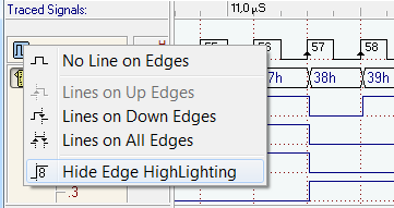
The menu is the same one that allows you to define the choice concerning the Time References. If the number is too big to be represented, isshortened, adding an apostrophe. For example, 34567 can be abbreviated, depending on the available space, as '567, '67 or '7, so that the progression of the numbering be always readable.
Defined a new command to generate a "quality" time diagram template (in black and white), useful for the preparation on paper of exercises and examination texts (see the example below):
The diagram includes clock cycle numbering, and a grid for entering the state code. The diagram is saved as a PNG or BMP lossless image ( "normal" or "rotated" of 90 degrees counterclockwise). The diagram contents are the same that are currently visualized in the Timing Diagram window. For instance, if a track is "expanded" in sub-tracks, these ones will appear in the diagram image.
Moreover, if you execute the simulation, and then you generate again the image, you'll get also the simulation results, as expected:
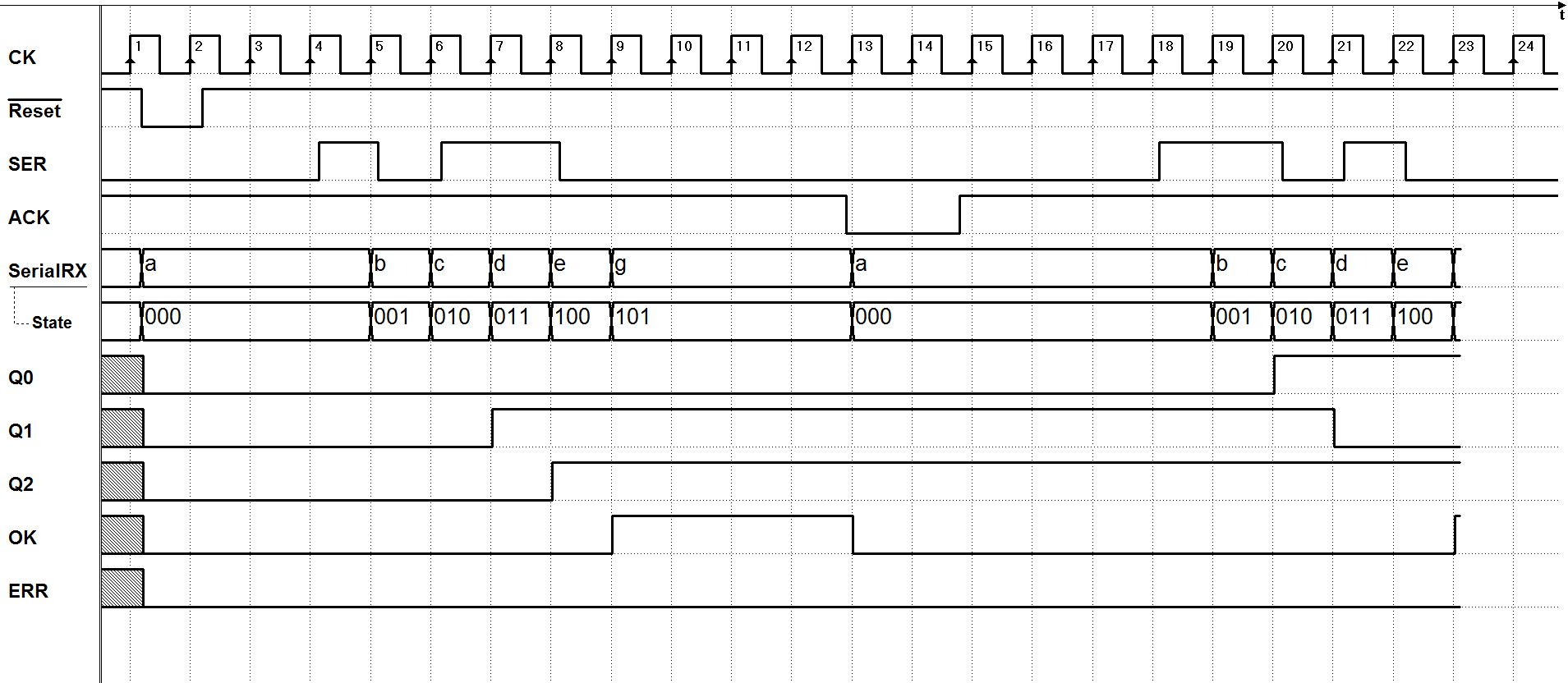
In this way, the same command can be used to obtain both the template for the text of the exercise and the one for publishing the solution.
This new command ('Save Diagram (high-quality)') coexists with the previous one ('Copy Timing Diagram'), that simply saves on the clipboard the dump of the diagram. The new command is accessible via the same icon of the previous version but, now, the click on the icon produces the descent of the following menu:
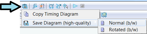
The file name can be changed by the user, but it is constructed, by default, combining the following strings: "TimingDiagram_" + <circuit filename> + (<test sequence name>).
The "Value Cursor" and the "Time Cursor" are compatible with the generation of the Timing Diagram image, while the presence of the "Magnifier" not. For this reason, if the "Magnifier" is active, it is temporarily closed and then re-opened; in the meanwhile, the diagram image is generated. The user will continue to see the "Magnifier" on the screen, but in the image it will be absent.
Fixed a bug regarding the "Value" cursor, in the Timing Diagram. In the case of multi-wired output devices, the value of the sub-track did not display properly. Now, both main- and sub-tracks "values" are correctly handled.
Fixed a bug of the "old" hexadecimal display (in the obsolete library), that in timing simulation gave a fatal error (it was due to an initialization fault at the start of the simulation time).
 Deeds-FsM
 A few tool-bar hints have been fixed: "State", "Decision", "Conditional Output":
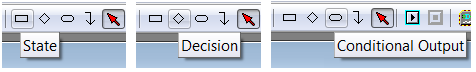
Now, on the status bar will appear, respectively:
"Add a new State box", "Add a new Decision box", "Add a new Conditional Output box".
As in the Deeds-DcS, also in the Deeds-FsM we added support to correct the names given to the VHDL file and its entities, to be all VHDL compliant (although obtained from the original file name).